|
|
 |
Creating A Schmitt Trigger Input Digital I/O Interface Model
Digital I/O models capture the electrical information common to the IC technology and
circuit techniques used to design and build them. A typical digital family will only
have a few I/O models. The only difference in the I/O models within a digital family
is to account for the different circuits employed at the input or output such as
open-collector outputs or Schmitt trigger inputs. An article in the
Winter 2003 newsletter
described creating the standard digital I/O model for the 74LV-A family from Texas
Instruments. A second article in the
Spring 2003 newsletter
described how to create an open drain output digital I/O model for the same family. This
article will expand on the previous articles in describing how to create a Schmitt trigger
input digital I/O model for the 74LV-A family.
The Schmitt trigger input digital I/O model differs from the standard digital I/O model
only in its analog to digital modeling, so the digital to analog portion of the model
will be exactly the same as the standard model. This article will emphasize the
differences between the two models which will be in the digital output device model
statement, the AtoD interface subcircuit, and the I/O model statement. To understand the
basics of the digital I/O model, read the
Winter 2003 article.
Digital Output Device (O Device) Model Statement
The digital output device is the component that converts an analog voltage into its
equivalent digital state for when an analog node is connected to a digital input. It does
the conversion by assigning voltage ranges to the digital states. If the analog input
voltage falls within a range, the output will be the corresponding digital state. These
voltage ranges are defined in the model statement for the O device. The Schmitt trigger
input will need only one O device model statement since it will not have any of the rise,
fall, or unknown intermediate states. The O model statement for the 74LV-A Schmitt trigger
input is:
.model DO74LV-A_ST doutput (
+ s0name="0" s0vlo=-.5 s0vhi=2
+ s1name="1" s1vlo=1.35 s1vhi=7)
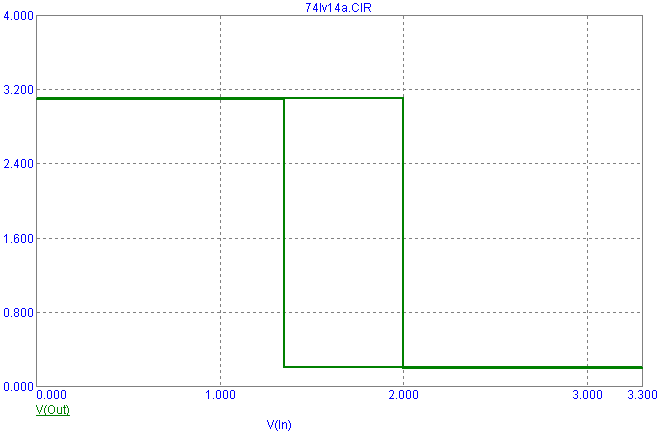
The DO74LV-A_ST model simulates the hysteresis of the Schmitt trigger through the
overlapping voltage ranges of the s0vhi and s1vlo parameters. The hysteresis value is
determined by the difference between the two: s0vhi - s1vlo. The s0vhi parameter is
defined from the VT+ positive going threshold voltage, and the s1vlo parameter is defined
from the VT- negative going threshold voltage. The s0vlo and s1vhi parameters take their
values from the minimum and maximum input voltage ranges, respectively.
The hysteresis occurs due to the progressive search that is deployed when determining the
digital state for the input voltage. The search starts at the current state range. If
the voltage is outside this range, it tries the next possible range. If it fails on the
last specified range, it will wrap around to the first range again. If it fails all of
the ranges, it will choose the range with the nearest voltage match. For example, if the
input voltage is currently at 1V, the model will assign a 0 state to the digital input.
The input voltage would then need to rise to over 2V before it leaves the voltage range
defined for the 0 state. At that point, the model will assign a 1 state to the digital
input. Subsequently, the input voltage would have to drop below 1.35V before it will exit
the voltage range for the 1 state and return to the voltage range of the 0 state.
AtoD Interface Subcircuit
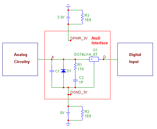
The AtoD interface subcircuit is the actual component that is placed between an analog
component and a digital input internally when an analysis is entered. For the 74LV-A
Schmitt trigger input, the subcircuit is as follows:
.subckt ATOD_LV-A_ST A D DPWR_3V DGND_3V
+ params: CAPACITANCE=0
O1 A DGND_3V DO74LV-A_ST DGTLNET=D IO_LV-A_ST
C1 A DGND_3V {CAPACITANCE+.1P}
D1 DGND_3V A D74
R1 A 1 170
C2 1 DGND_3V 1p
.ends
The AtoD subcircuit for the Schmitt trigger input model contains the same circuit structure
as the standard model. The only differences between the Schmitt trigger and the standard
subcircuits are in the name of the subcircuit and the models that are referenced within
the subcircuit. Note that the O1 AtoD device references the DO74LV-A_ST model that was
just created and the IO_LV-A_ST I/O model that will be created in the next section. Due
to the CMOS process used to create these devices, the analog circuitry of the input is
dominated by the ESD protection scheme so the Schmitt trigger input uses the same circuitry
as the standard model. The 74LV-A family has no current paths to the power node in order
to be able to interface directly with TTL devices, so the power node in the AtoD interface
subcircuit will be left floating. The power node is still available as it is frequently
used in many digital families, and it is displayed as unconnected in the schematic
equivalent of the AtoD interface shown below.
|

|
I/O Model Statement
The I/O model provides the information necessary to determine the output strength when
devices are wire-ored together and to create the interface circuits when the digital
part is connected to an analog part. The model brings together all of the interface
subcircuits and models for use by a digital component. The Schmitt trigger I/O model
statement for the 74LV-A family appears as follows:
.model IO_LV-A_ST uio (
+ DRVH=130 DRVL=130
+ INLD=2.1p
+ ATOD1="ATOD_LV-A_ST" ATOD2="ATOD_LV-A_ST"
+ ATOD3="ATOD_LV-A_ST" ATOD4="ATOD_LV-A_ST"
+ DTOA1="DTOA_LV-A" DTOA2="DTOA_LV-A"
+ DTOA3="DTOA_LV-A" DTOA4="DTOA_LV-A"
+ TSWHL1=2.80n TSWHL2=2.80n
+ TSWHL3=2.80n TSWHL4=2.80n
+ TSWLH1=2.01n TSWLH2=2.01n
+ TSWLH3=2.01n TSWLH4=2.01n
+ DIGPOWER="DIGIFPWR_3V")
The Schmitt trigger input I/O model retains many of the same values as the standard
model. Most of the parameters reference the DtoA or power supply characteristics of
the model and will not change.
The INLD capacitance parameter defines the input load capacitance in order to compute
the optional loading delay through the device to account for excessive capacitive
loading on the node caused by high fan-out. In this case, it is defined with an
average input capacitance value of 2.1pF for the Schmitt trigger devices within the
74LV-A family.
The ATOD1 through ATOD4 parameters define the names of the analog to digital interface
subcircuits that will be called when a digital input is connected to an analog component.
These parameters have all been defined with the 'ATOD_LV-A_ST' Schmitt trigger AtoD
interface subcircuit created previously. This AtoD subcircuit is applicable for all four
levels, so all four parameters share the same value.
Example 74LV-A Family Digital Device
The 74LV14A inverter subcircuit below shows how the I/O model is referenced in an actual
device.
.SUBCKT 74LV14A 1A 1Y
+ optional: DPWR_3V=$G_DPWR_3V DGND_3V=$G_DGND_3V
+ params: MNTYMXDLY=0 IO_LEVEL=0
U1 inv DPWR_3V DGND_3V
+ 1A 1Y
+ DLY_LV14 IO_LV-A_ST MNTYMXDLY={MNTYMXDLY} IO_LEVEL={IO_LEVEL}
.model DLY_LV14 ugate (tplhTY=9.6ns tplhMX=16.3ns tphlTY=9.6ns tphlMX=16.3ns)
.ENDS 74LV14A
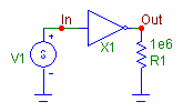
Note that the inverter device within the subcircuit uses IO_LV-A_ST as its I/O model
name. The 74LV14A inverter is tested in the circuit configuration shown below. A 3.3V
triangle wave is placed at the input of the inverter. The resistor lets Micro-Cap plot
the output as an analog voltage. The simulation of the circuit below shows the
hysteresis capability of the model.
|

|

|
|
|
|
|


