|
|
 |
Creating An Open Drain Output Digital I/O Interface Model
Digital I/O models capture the electrical information common to the IC
technology and circuit techniques used to design and build them. A
typical digital family will only have a few I/O models. The only
difference in the I/O models within a digital family is to account for
the different circuits employed at the input or output such as
open-collector outputs or Schmitt-trigger inputs. An
article in the Winter 2003
newsletter described creating the standard digital I/O model
for the 74LV-A family from Texas Instruments. This article will expand
on the previous article in describing how to create an open drain output
digital I/O model for the 74LV-A family.
The open drain output digital I/O model differs from the standard
digital I/O model only in its digital to analog modeling, so the analog
to digital portion of the model will be exactly the same as the standard
model. This article will emphasize the differences between the two
models which will be in the digital input device model statement, the
DtoA interface subcircuit, and the I/O model statement. To understand
the basics of the digital I/O model, read the Winter 2003 article.
Digital Input Device (N Device) Model Statement
The digital input device is the device within the interface that converts a digital output
node to its analog equivalent. It does the conversion by translating the digital states
to impedance changes on the analog side. Two resistors (RLO and RHI) are placed in a
voltage divider configuration between the power and ground nodes of the digital device.
These resistors determine the equivalent analog voltage of the digital output. The model
statement for the N device defines the values of the resistors for each digital state, and
the switching time between the old resistance and the new resistance when a state change
occurs. The model statement for the open drain output N device in the 74LV-A family is:
.model DIN74LV-A_OD dinput (
+ s0name="0" s0tsw=3.4n s0rlo=31.9 s0rhi=494.5 ;@30ohms, .2V
+ s1name="1" s1tsw=3.4n s1rlo=1Meg s1rhi=1Meg
+ s2name="F" s2tsw=3.4n s2rlo=58.1 s2rhi=73.2 ;@32.4 ohms, 1.46V
+ s3name="R" s3tsw=3.4n s3rlo=58.1 s3rhi=73.2 ;@32.4 ohms, 1.46V
+ s4name="X" s4tsw=3.4n s4rlo=58.1 s4rhi=73.2 ;@32.4 ohms, 1.46V
+ s5name="Z" s5tsw=3.4n s5rlo=1Meg s5rhi=1Meg)
Since the open drain output only affects the 1 and Z states of a digital component, the
0, F, R, and X states will retain the same values as they had in the standard model. The
1 state has its RHI and RLO resistances defined arbitrarily with values of 1Meg. The
resistance values are defined with a high value in order to minimize their impact on the
pullup resistor that is typically attached to the output of an open drain device. The Z,
high impedance, state is already defined with high resistance values, but the switching
time should be set to the same switching time as is defined for the 1 state. For the
74LV-A family, the switching times were already the same so no change is needed.
DtoA Interface Subcircuit
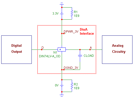
The DtoA interface subcircuit is the actual component that is placed between a digital
output and an analog component internally when an analysis is entered. For the open
drain output model, the subcircuit is as follows:
.subckt DTOA_LV-A_OD D A DPWR_3V DGND_3V
+ params: CAPACITANCE=0 DRVH=0 DRVL=0
N1 A DGND_3V DPWR_3V DIN74LV-A_OD DGTLNET=D IO_LV-A_OD
CLOAD A DGND_3V {CAPACITANCE+.1p}
.ends
The DtoA subcircuit for the open drain model contains the same circuit structure as the
standard model by having only an N (digital input) device and a load capacitor. The
only differences between the open drain and the standard subcircuits are in the name of
the subcircuit and the models that are referenced within the subcircuit. Note that the
N1 DtoA device references the DIN74LV-A_OD model that was just created and the IO_LV-A_OD
I/O model that will be created in the next section. There is no need to model the high
impedance element of the open drain output explicitly in this subcircuit since it is
specified in the N device model statement for both the 1 and Z states. The schematic
equivalent of the DtoA subcircuit interface appears below.
|

|
I/O Model Statement
The I/O model provides the information necessary to determine the output strength when
devices are wire-ored together and to create the interface circuits when the digital
part is connected to an analog part. The model brings together all of the interface
subcircuits and models for use by a digital component. The I/O model statement for
the 74LV-A open drain output appears as follows:
.model IO_LV-A_OD uio (
+ DRVH=1Meg DRVL=130
+ INLD=2.3p
+ ATOD1="ATOD_LV-A" ATOD2="ATOD_LV-A_NX"
+ ATOD3="ATOD_LV-A" ATOD4="ATOD_LV-A_NX"
+ DTOA1="DTOA_LV-A_OD" DTOA2="DTOA_LV-A_OD"
+ DTOA3="DTOA_LV-A_OD" DTOA4="DTOA_LV-A_OD"
+ TSWHL1=3.42n TSWHL2=3.42n
+ TSWHL3=3.42n TSWHL4=3.42n
+ TSWLH1=0.16n TSWLH2=0.16n
+ TSWLH3=0.16n TSWLH4=0.16n
+ DIGPOWER="DIGIFPWR_3V")
The open drain output I/O model retains some of the same values as the standard model.
The DRVL, INLD, ATOD1, ATOD2, ATOD3, ATOD4, and DIGPOWER parameters will all have the
same values. Most of these define the input characteristics or the power supply for
the device which do not change. The DRVL parameter stays the same since the open drain
output will only affect the high state output of the device.
The DRVH parameter is arbitrarily assigned the value of 1Meg. This parameter defines the
high state output strength that is used to resolve the output state when multiple digital
outputs are wire-ored together. With an open drain output, the drive strength is weak
and so is defined with a high resistance value. The open drain output devices are
typically dependent on pullup resistors to provide the drive resistance.
The DTOA1 through DTOA4 parameters define the names of the digital to analog interface
subcircuits that will be called when a digital output is connected to an analog
component. These parameters have all been defined with the 'DTOA_LV-A_OD' open drain
DtoA interface subcircuit created previously. This DtoA subcircuit is applicable for
all four levels, so all four parameters share the same value.
The TSWLH1 through TSWLH4 and TSWHL1 through TSWHL4 define the switching times for the
I/O model. The switching times are subtracted from the digital device's propagation
delay on outputs which are connected to analog components so that the analog signal at
the other side of the DtoA interface should reach the switching level just when the
digital device does at the stated delay. Since the same DtoA subcircuit is used for
all four cases in this family, the switching times will be the same for each level of
a transition.
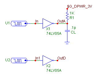
The switching time parameters in the I/O model are initially set to 0. To measure the
switching times, a schematic similar to the one below may be used. The schematic consists
of two separate circuits. The only difference between the two circuits is that the top
one has a minimal load capacitance of .1pF and a 1K pullup resistor whereas the bottom
circuit has no load at all. The 1K pullup resistor value in the top circuit was taken
from the waveform test circuits in the 74LV05A data sheet. The two digital stimulus
sources start in the zero state, at 100ns transition to the one state, and at 200ns
transition back to the zero state. These sources are fed into 74LV05A inverters which
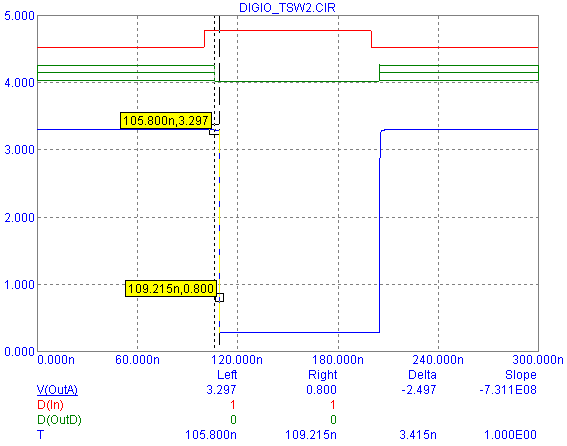
reference the IO_LV-A_OD I/O model. A transient analysis is run on this schematic
with the results displayed below. Three waveforms are plotted: D(In), D(OutD), and
V(OutA). D(In) is the digital input waveform from one of the stimulus sources. D(OutD)
is the digital output waveform of the inverter with no load. Note that for the D(OutD)
waveform, its high state is actually represented with a Z (high impedance state). This
occurs due to the high DRVH value in the I/O model, and the fact that there is no pullup
resistor on the output to drive the node to a 1 state. V(OutA) is the output voltage
waveform of the inverter with an analog load. The switching time is measured from the
point that the no-load output makes its transition to when the analog load output reaches
either the Vih or Vil value depending on the transition. For example, to measure the high
to low switching time, one cursor is placed at the point where the D(OutD) waveform has a
ZL transition, and the other cursor is placed at the point where the analog output reaches
its Vil voltage which in this case is .8V. The switching time is the time differential
between these two points which comes out to 3.42ns for the open drain model. Similarly,
for the low to high switching time, one cursor is placed at the LZ transition for D(OutD),
and the other cursor is placed at the point where the analog output reaches its Vih
voltage which is 2V for this model. The low to high switching time is measured at 0.16n.
The switching time parameters are then updated with these new values.
|

|

|
Example 74LV-A Open Drain Output Device
The 74LV05A inverter from the switching time measurement shows how the I/O model is
referenced in an actual device.
.SUBCKT 74LV05A 1A 1Y
+ optional: DPWR_3V=$G_DPWR_3V DGND_3V=$G_DGND_3V
+ params: MNTYMXDLY=0 IO_LEVEL=0
U1 inv DPWR_3V DGND_3V
+ 1A 1Y
+ DLY_LV05 IO_LV-A_OD MNTYMXDLY={MNTYMXDLY} IO_LEVEL={IO_LEVEL}
.model DLY_LV05 ugate (tplhTY=4.7ns tplhMX=10.6ns tphlTY=5.8ns tphlMX=10.6ns)
.ENDS 74LV05A
Note that the inverter device within the subcircuit uses IO_LV-A_OD as its I/O model
name.
|
|
|
|
|


