|
|
 |
Creating A Digital I/O Interface Model
Digital I/O models capture the electrical information common to the IC technology and circuit techniques
used to design and build them. A typical digital family will only have a few I/O models. The only
difference in the I/O models within a digital family is to account for the different circuits employed
at the input or output such as open-collector outputs or Schmitt-trigger inputs. The I/O models provide
the information necessary to determine the output strength when devices are wire-ored together, and to
create the interface circuits when the digital part is connected to an analog part. This article will
describe the steps taken to create an I/O interface for the 74LV-A low voltage logic family at its
typical power supply voltage of 3.3V.
Power Supply Subcircuit
The digital power supply subcircuit defines the default power supply for the logic family when the
supply is not specified in a schematic. This subcircuit is called whenever an AtoD or DtoA interface is
required. Multiple logic families can use the same power supply subcircuit if it is applicable. For
the 74LV-A family, the nominal voltage supply for the VCC pin is 3.3V. The subcircuit below defines the
power supply.
.subckt DIGIFPWR_3V AGND
+ optional: DPWR_3V=$G_DPWR_3V DGND_3V=$G_DGND_3V
+ params: VOLTAGE=3.3 REFERENCE=0
V1 DPWR_3V AGND {VOLTAGE}
R1 DPWR_3V AGND 1E9
V2 DGND_3V AGND {REFERENCE}
R2 DGND_3V AGND 1E9
R3 AGND 0 1m
.ends
The subcircuit basically consists of two batteries with a large resistor in parallel with each. The
batteries are defined by the VOLTAGE and REFERENCE parameters, which in this case, have been defined as
3.3V and 0V respectively. The optional nodes, DPWR_3V and DGND_3V, define the power and ground node
names that will be used throughout the I/O model and in components that reference this I/O model.
Digital Input Device (N Device) Model Statement
The digital input device is the device within the interface that converts a digital output node to its
analog equivalent. It does the conversion by translating the digital states to impedance changes on the
analog side. Two resistors (RLO and RHI) are placed in a voltage divider configuration between the power
and ground nodes of the digital device. These resistors determine the equivalent analog voltage of the
digital output. The model statement for the N device defines the values of the resistors for each
digital state, and the switching time between the old resistance and the new resistance when a state
change occurs. The model statement for the standard N device in the 74LV-A family is:
.model DIN74LV-A dinput (
+ s0name="0" s0tsw=3.4n s0rlo=31.9 s0rhi=494.5 ;@30ohms, .2V
+ s1name="1" s1tsw=3.4n s1rlo=578.2 s1rhi=37.3 ;@35 ohms, 3.1V
+ s2name="F" s2tsw=3.4n s2rlo=58.1 s2rhi=73.2 ;@32.4 ohms, 1.46V
+ s3name="R" s3tsw=3.4n s3rlo=58.1 s3rhi=73.2 ;@32.4 ohms, 1.46V
+ s4name="X" s4tsw=3.4n s4rlo=58.1 s4rhi=73.2 ;@32.4 ohms, 1.46V
+ s5name="Z" s5tsw=3.4n s5rlo=1Meg s5rhi=1Meg)
The N device model statement defines three parameters for each state: the switching time (tsw), the low
resistance (rlo), and the high resistance (rhi). The switching time defines the amount of time it takes
for the resistors to transition to their new value for the state. The switching times should be close to
the typical propagation delay for the family. The main I/O model has parameters that compensate for these
switching times, so that the resistance values reach their new value at approximately the same time as the
state changes at the output. A 0-R-1 transition will produce a 6.8ns switching time for this model.
The resistance values for each state are determined by the V-I curves for the family. For the 0 state,
the slope of the VOL vs IOL curve is taken to obtain a resistance (RSL). The RSL resistance is then
used to calculate the RLO and RHI resistors in the model statement through the two following equations:
VO = (VPWR*RLO)/(RLO + RHI)
RSL = (RLO*RHI)/(RLO + RHI)
VPWR is the power supply for the family which in this case is 3.3V. VO is the typical low state output
voltage at a power supply of 3.3V which is .2V for this family. RSL was determined to be 30 ohms from
the VOL vs IOL curve, so the resulting resistances for the 0 state are RLO=31.9 and RHI=494.5. For the
1 state, the same equations are used except that the RSL is determined by the slope of the VOH vs IOH
curve, and VO is the typical high state output voltage which is 3.1V for this family. With the RSL
resistance measured at 35 ohms, the resistances for the 1 state are calculated at RLO=578.2 and
RHI=37.3.
For the F, R, and X states, the above equations are also used. These three states will be arbitrarily
represented as a midpoint between the 0 and 1 states. The RSL resistance for these states is determined
by taking the square root of the product of the RSL resistances determined for the 0 and 1 state as
follows:
RSL = SQRT(RSL(0) * RSL(1))
The VO voltage is defined as the voltage exactly halfway between the minimum high output voltage and the
maximum low output voltage. For the 74LV-A family, the RSL comes out to 32.4 ohms and the output voltage
is determined to be 1.46V. These values produce resistances of RLO=58.1 and RHI=73.2.
For the Z state, the RHI and RLO parameters have been arbitrarily assigned the value of 1Meg to represent
the high impedance of the state, and the switching time is set to the same value as the F, R, and X
states.
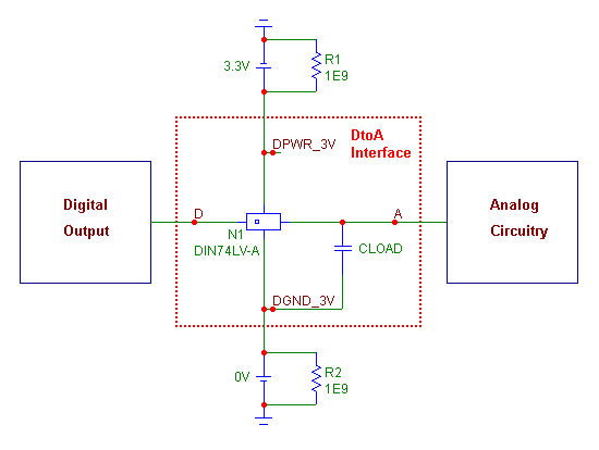
DtoA Interface Subcircuit
The DtoA interface subcircuit is the actual component that is placed between a digital output and an
analog component internally when an analysis is entered. For the 74LV-A family, the subcircuit is as
follows:
.subckt DTOA_LV-A D A DPWR_3V DGND_3V
+ params: CAPACITANCE=0 DRVH=0 DRVL=0
N1 A DGND_3V DPWR_3V DIN74LV-A DGTLNET=D IO_LV-A
CLOAD A DGND_3V {CAPACITANCE+.1p}
.ends
The DtoA subcircuit consists of only two components, an N device, referencing the model statement just
created, and a capacitor. The power and ground nodes throughout the subcircuit are given the same name
as the power and ground nodes in the power supply subcircuit. The I/O model specification for the N
device is defined with the name of the full I/O model, IO_LV-A, that will be created further along in
this article. The DRVH and DRVL parameters are the high state and low state impedances used to
determine output strength. The CAPACITANCE parameter is used to increase the propagation delay through
the device to account for excessive capacitive loading on the node caused by high fan-out. These
parameters will be overwritten by the DRVH, DRVL, and OUTLD parameters available in the IO_LV-A model,
so they are set to 0 for the subcircuit. The schematic equivalent of the DtoA subcircuit interface
appears in the figure below.
|

|
Digital Output Device (O Device) Model Statements
The digital output device is the component that converts an analog voltage into its equivalent digital
state for when an analog node is connected to a digital input. It does the conversion by assigning
voltage ranges to the digital states. If the analog input voltage falls within a range, the output
will be the corresponding digital state. These voltage ranges are defined in the model statement for
the O device. The 74LV-A family will have two O device model statements. One model will contain all
the intermediate states such as R, F, and X along with the 0 and 1 states, and the other will be a
simplified model that contains only the 0 and 1 states. This is typical of all of the families that
are included with Micro-Cap. The model that is actually used in simulation is dependent on the
Global Setting DIGIOLVL parameter which specifies which of the four DtoA and AtoD subcircuit interfaces
to use. The two O model statements for the 74LV-A family are:
.model DO74LV-A_NX doutput (
+ s0name="0" s0vlo=-.5 s0vhi=1.65
+ s1name="1" s1vlo=1.65 s1vhi=7)
.model DO74LV-A doutput (
+ s0name="X" s0vlo=.8 s0vhi=2
+ s1name="1" s1vlo=2 s1vhi=7
+ s2name="F" s2vlo=1.6 s2vhi=2
+ s3name="F" s3vlo=.8 s3vhi=1.7
+ s4name="X" s4vlo=.8 s4vhi=2
+ s5name="0" s5vlo=-.5 s5vhi=.8
+ s6name="R" s6vlo=.8 s6vhi=1.7
+ s7name="R" s7vlo=1.6 s7vhi=2)
To determine which range contains the input voltage level, a progressive search is employed. The search
starts at the current state range. If the voltage is outside this range, it tries the next possible
range. If it fails on the last specified range, it will wrap around to the first range again. If it
fails all of the ranges, it will choose the range with the nearest voltage match.
The DO74LV-A model represents the more complex AtoD interface. The 1 state defined on the s1 line uses
the high level input voltage as its low voltage and the maximum input voltage as its high voltage. The
0 state defined on the s5 line uses the minimum input voltage as its low voltage and the low level input
voltage as its high voltage. The R, F, and X states are defined within the voltage range set by the low
level input voltage and the high level input voltage. The order that the states are defined in is also
important due to the nature of the progressive search. Typically, the first state defined should be an
X (unknown) state. This is the range that the simulation will first test. If the input voltage at
that point is between .8V and 2V, it doesn't know whether it should be at a 0 or 1 state and will produce
a resulting X state. The next state was chosen to be a 1 state. Following the 1 state is a combination
of F (fall), F, and X states. The logic behind this combination is that it forces the analog input to
have a fairly smooth transition between the 1 and 0 state. If the input voltage ramps linearly down
from 2.5V to .5V, the digital output will go from the 1 state, to the first F state, to the second F
state, and then to the 0 state. In the simulation, the user will just see a 1-F-0 transition. If the
input analog voltage were to oscillate on the way down such as going from 2.5V to 1.5V back up to 1.8V
and then down to .5V, the digital output will go from the 1 state, to the first F state, to the second
F state, to the following X state, and then to the 0 state. In the simulation, the user will see a
1-F-X-0 transition. The X state is present to show that oscillation around the input threshold voltage
will produce an ambiguous situation. This is the reason the F state was divided into two separate ranges
around the input threshold voltage. The 0, R (rise), and R combination as the final three states are
defined with the same logic in mind. This combination wraps around to use the s0 X state as its unknown
state in case of oscillation.
The DO74LV-A_NX model represents the simple AtoD interface. The 0 state range is defined between the
minimum input voltage and the input threshold voltage, and the 1 state range is defined between the
input threshold voltage and the maximum input voltage. The order of the states in this model is
meaningless since there are only two voltage ranges to sample from.
AtoD Interface Subcircuits
The AtoD interface subcircuit is the actual component that is placed between an analog component and
a digital input internally when an analysis is entered. Two AtoD subcircuits will be created for this
model in order to take advantage of both of the digital output device model statements created in the
previous section. For the 74LV-A family, the subcircuits are as follows:
.subckt ATOD_LV-A A D DPWR_3V DGND_3V
+ params: CAPACITANCE=0
O1 A DGND_3V DO74LV-A DGTLNET=D IO_LV-A
C1 A DGND_3V {CAPACITANCE+.1P}
D1 DGND_3V A D74
R1 A 1 170
C2 1 DGND_3V 1p
.ends
.subckt ATOD_LV-A_NX A D DPWR_3V DGND_3V
+ params: CAPACITANCE=0
O1 A DGND_3V DO74LV-A_NX DGTLNET=D IO_LV-A
C1 A DGND_3V {CAPACITANCE+.1P}
D1 DGND_3V A D74
R1 A 1 170
C2 1 DGND_3V 1p
.ends
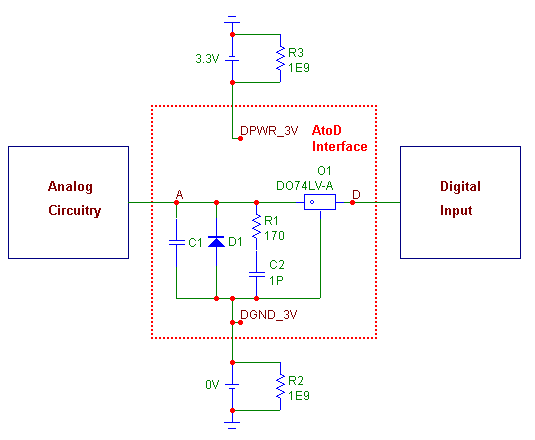
The only differences in the two subcircuits are in the subcircuit name and in the model name that the O
device references. This AtoD subcircuit consists of five components. The O device, referencing one of
the model statements from the previous section, is the heart of the subcircuit and performs the AtoD
conversion. The power and ground nodes throughout the subcircuit are given the same name as the power
and ground nodes in the power supply subcircuit. The I/O model specification for the O device is
defined with the name of the full I/O model, IO_LV-A, that will be created next. The CAPACITANCE
parameter is used to increase the propagation delay through the device to account for excessive
capacitive loading on the node caused by high fan-out and is modelled by the C1 capacitor in the
subcircuit. This parameter will be overwritten by the INLD parameter available in the IO_LV-A model,
so it is set to 0 for the subcircuit. The rest of the components are used to model the typical
analog input circuitry of the digital component. For the 74LV-A family, which is created through a
CMOS process, the input is dominated by the ESD protection scheme which is modelled by the D1
diode, R1 resistor, and C2 capacitor. The 74LV-A family has no current paths to the power node in
order to be able to interface directly with TTL devices, so the power node in the AtoD interface
subcircuit will be left floating. The power node is still available as it is frequently used in
many digital families, and it is displayed as unconnected in the schematic equivalent of the AtoD
interface shown below.
|

|
I/O Model Statement
The I/O model provides the information necessary to determine the output strength when devices are
wire-ored together and to create the interface circuits when the digital part is connected to an
analog part. The model brings together all of the subcircuits and models defined in the previous
sections for use by a digital component. The I/O model statement for the 74LV-A family appears
as follows:
.model IO_LV-A uio (
+ DRVH=130 DRVL=130
+ INLD=2.3p
+ ATOD1="ATOD_LV-A" ATOD2="ATOD_LV-A_NX"
+ ATOD3="ATOD_LV-A" ATOD4="ATOD_LV-A_NX"
+ DTOA1="DTOA_LV-A" DTOA2="DTOA_LV-A"
+ DTOA3="DTOA_LV-A" DTOA4="DTOA_LV-A"
+ TSWHL1=2.80n TSWHL2=2.80n
+ TSWHL3=2.80n TSWHL4=2.80n
+ TSWLH1=2.01n TSWLH2=2.01n
+ TSWLH3=2.01n TSWLH4=2.01n
+ DIGPOWER="DIGIFPWR_3V")
DRVH and DRVL are the high state and low state impedances used to determine the output strength. The
output strength is used to resolve the output state when a digital output is connected to other digital
outputs. For the 74LV-A family, the line drive impedance is defined as 130 ohms for both the high and
low states.
The INLD parameter defines the input load capacitance. It is used to compute the optional loading
delay through the device to account for excessive capacitive loading on the node caused by high
fan-out. In this instance, a capacitance of 2.3pF was chosen by selecting an average input capacitance
value from the products in the family.
The ATOD1 through ATOD4 parameters define the names of the analog to digital interface subcircuits that
will be called when an analog component is connected to a digital input. The actual subcircuit that
will be chosen for an analysis will be determined by the IO_LEVEL parameter within a component that
references the I/O model or by the Global Setting parameter, DIGIOLVL. If the value of DIGIOLVL is
set to 2, then the subcircuit defined by the ATOD2 parameter will be used. Note that the simpler
AtoD models have been defined as levels 2 and 4, whereas the more complex models are defined with
levels 1 and 3. The DTOA1 through DTOA4 parameters define the names of the digital to analog interface
subcircuits that will be called when a digital output is connected to an analog component. These
parameters act in the same manner as the ATOD parameters. Since only one DtoA model has been defined
for the family, that model is specified for all four parameters.
The TSWLH1 through TSWLH4 and TSWHL1 through TSWHL4 define the switching times for the I/O model. The
switching times are subtracted from the digital device's propagation delay on outputs which are connected
to analog components. The purpose is to compensate for the time it takes the DtoA interface circuit to
switch. By compensating in this way, the analog signal at the other side of the DtoA interface should
reach the switching level just when the digital device does at the stated delay. If a switching time is
greater than the device's stated delay, a delay of zero will be used. The IO_LEVEL parameter within a
component or the DIGIOLVL Global Setting parameter also determines which of the four switching times it
will use here also. Since the same DtoA subcircuit is used for all four cases in this family, the
switching times will be the same for each level of a transition.
|

|
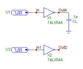
The switching time parameters in the I/O model are initially set to 0. To measure the switching times,
a schematic similar to the one above may be used. The schematic consists of two separate circuits.
The only difference between the two circuits is that the top one has a minimal load capacitance of .1pF
whereas the bottom circuit has no load at all. The two digital stimulus sources start in the zero
state, at 100ns transition to the one state, and at 200ns transition back to the zero state. These
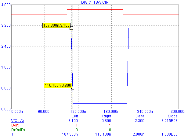
sources are fed into 74LV04A inverters which reference the I/O model that was just created. A transient
analysis is run on this schematic with the results displayed below. Three waveforms are plotted: D(In),
D(OutD), and V(OutA). D(In) is the digital input waveform from one of the stimulus sources. D(OutD) is
the digital output waveform of the inverter with no load, and V(OutA) is the output voltage waveform of
the inverter with a capacitive load. The switching time is measured from the point that the no-load
output makes its transition to when the capacitive load output reaches either the Vih or Vil value
depending on the transition. For example, to measure the high to low switching time, one cursor is
placed at the point where the D(OutD) waveform has a HL transition, and the other cursor is placed at
the point where the analog output reaches its Vil voltage which in this case is .8V. The switching time
is the time differential between these two points which comes out to 2.80ns for the 74LV-A model.
Similarly, for the low to high switching time, one cursor is placed at the LH transition for D(OutD), and
the other cursor is placed at the point where the analog output reaches its Vih voltage which is 2V for
this family. The low to high switching time is measured at 2.01ns. The switching time parameters are
then updated with these new values.
|

|
The DIGPOWER parameter specifies the name of the power supply subcircuit to be used when an AtoD or DtoA
interface is required. The parameter is defined with the name of the DIGIFPWR_3V subcircuit that was
created at the beginning of the article.
Example 74LV-A Family Digital Device
The 74LV04A inverter from the switching time measurement shows how the I/O model is referenced in an
actual device.
.SUBCKT 74LV04A 1A 1Y
+ optional: DPWR_3V=$G_DPWR_3V DGND_3V=$G_DGND_3V
+ params: MNTYMXDLY=0 IO_LEVEL=0
U1 inv DPWR_3V DGND_3V
+ 1A 1Y
+ DLY_LV04 IO_LV-A MNTYMXDLY={MNTYMXDLY} IO_LEVEL={IO_LEVEL}
.model DLY_LV04 ugate (tplhTY=7.3ns tplhMX=10.6ns tphlTY=7.3ns tphlMX=10.6ns)
.ENDS 74LV04A
Note that the power and ground nodes (for both the optional nodes and the inverter supply nodes) use
the same name as those in the digital power supply subcircuit referenced by the I/O model, and the
inverter device within the subcircuit uses IO_LV-A as its I/O model name.
|
|
|
|
|


