|
|
 |
Spark-Gap Macro
The spark-gap arrestor, also known as the surge arrestor, is used to block transient surges such as from lightning strikes. The spark gap is filled with an inert gas and uses two electrodes that provide a very high impedance to the circuit, and as long as the voltage across it is less than the striking voltage, the current is approximately zero. When a surge hits the arrestor, the two electrodes act as a short circuit. The voltage across the spark-gap then drops to its glow voltage and if the current continues to increase, drops down to its arc voltage. The spark-gap will continue to conduct until the current through it falls below a sustaining value. Spark-gaps can be found in such applications as aircraft ignition systems, oil burners, and magnetron protection.
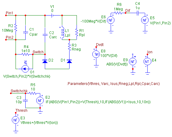
The spark-gap macro circuit appears below (sparkgap.cir - MC5 V2 only, Save As to your disk and then load in MC5). This macromodel was derived based on an article by Christophe Basso titled "SPICE model simulates spark-gap arrestor" which appears in the July 3, 1997 issue of EDN. This model does not simulate the glow transition of a spark-gap. There are seven parameters for this macro. The parameters are defined as follows:
VTHRES - Voltage at which the spark-gap strikes
VARC - Voltage across the spark-gap once struck
ISUS - Sustaining current under which the arc is stopped
RNEG - Negative resistance once struck
LPL - Lead inductance
RPL - Flux loss associated with LPL
CPAR - Gap capacitance
CARC - Arc capacitance
|

|
The macro has two operating states: off and on. In its off state, the macro only has a small leakage current flowing through it, and the model is represented by the R2 resistor and C1 capacitor. The R2 resistor places a 10Meg ohm resistance across the two pins of the spark gap, and the C1 capacitor models the gap capacitance, defined by the CPAR parameter, in the off state.
When the voltage across the spark-gap reaches the striking voltage, the spark-gap transitions to its on state and begins conducting. At this point, the macro is essentially comprised of the L1 inductor, the C2 capacitor, the R1 and R3 resistors, and the D1 and D2 diodes. The L1 inductor and the R1 resistor simulate the lead inductance, defined by the LPL parameter, and the flux loss corresponding to the lead inductance, defined by the RPL parameter. The capacitance of the macro is modelled by the C2 capacitor which simulates the arc capacitance as defined by the CARC parameter. The R3 resistor models the series resistance as defined by the RNEG parameter. The D1 and D2 diodes are back to back zener diodes which have the following model statement residing in the text area:
.MODEL DCLAMP D (BV=VARC)
where the parameter VARC defines the breakdown voltage of each of the diodes. When the spark-gap is conducting, the voltage of the spark-gap will be controlled by the zener voltage VARC.
The state of the spark-gap is controlled through the switch between the nodes Switch and Pin2 that is comprised of the R4 resistor and G1 nonlinear function current (NFI) source. When the G1 NFI current is small, the 1E10 ohms of the R4 resistor act as an open circuit. Otherwise, the G1 source shorts the R4 resistor causing the back to back zener diode network to connect across the spark-gap pins. The G1 source has its VALUE attribute defined as:
V(Switch,Pin2)*V(Switchchk)
which multiplies the voltage across itself by the voltage produced at the node Switchchk. The voltage at node Switchchk is determined by a number of factors such as the dv/dt of the voltage applied to the spark-gap, the voltage across the spark-gap, and the current through the spark-gap. Nonlinear function voltage (NFV) sources and a nonlinear table VofV source are used to compute these factors in order to control the switch. The E5 NFV source has its VALUE attribute defined as:
V(Pin1,Pin2)
which produces the value of the voltage across the spark-gap. This voltage is fed into a classic differentiator consisting of the C4 capacitor, the R6 resistor, and the E6 NFV source. The E6 NFV source has its VALUE attribute defined as:
-100Meg*V(Dif)
In calculating the standard loop equations for that differentiator, the voltage at node Dif will be a scaled equivalent of the dv/dt of the voltage across the spark-gap. The basic loop equation is as follows:
V(Dif) = I*R6 - 100Meg*V(Dif)
where the V(Dif) on the left hand side is swamped out by the 100Meg*V(Dif) on the right hand side. Substituting 1Meg for R6, the equation reduces to:
100Meg*V(Dif) = 1Meg*I
V(Dif) = I/100
Due to the small value of V(Dif), the voltage across the capacitor is essentially equal to the voltage from E5 so the current can be determined by the equation:
I = C*d(V(E5))/dt
which plugged into the V(Dif) equation above gives the final result as approximately:
V(Dif) = 1E-8*d(V(E5))/dt
This resulting voltage at node Dif is subsequently fed into the E8 NFV source. The E8 source has its VALUE attribute defined as:
100*V(Dif)
which converts the voltage at node Dif into a voltage equivalent to the dv/dt of the voltage across the spark-gap in units of V/us. For example, if the voltage at node Dvdt is 1 volt, then the dv/dt of the voltage across the spark-gap is 1V/us. The E9 NFV source with its VALUE attribute defined as:
ABS(V(Dvdt))
takes the absolute value of the voltage at node Dvdt and uses this value as the input to the E4 nonlinear table source. The E4 source has its TABLE attribute defined as:
(0,0) (1U,.5565M) (10M,1M) (100M,86M) (1,217M) (10,521M) (100,956M)
This table source produces a corresponding voltage at node Ion that is dependent on the rate of the dv/dt of the voltage across the spark-gap. For example, if the dv/dt of the spark-gap voltage is 1V/us, then the table source will produce a voltage of 217mV. Currently, the table values are only set to handle transients of up to 100V/us. The table values were taken from the VIgnition/dv/dt curves of a spark-gap data sheet. This voltage is then used in the E3 NFV source which has its VALUE attribute defined as:
Vthres+(Vthres*V(Ion))
This source produces the actual striking voltage used by the spark-gap at node Thresh. The ignition voltage is determined from the VTHRES parameter and the voltage at node Ion. The offset produced by the Vthres*V(Ion) product represents the fact that the gas within the spark-gap needs a certain amount of time to ionize so that faster transients will reach a higher voltage before the gas is ionized and the spark-gap trips. Finally, the E2 NFV source produces the voltage at Switchchk that controls the G1 source. The R5 resistor and C3 capacitor provide a slight delay for the voltage from the E2 source. The E2 NFV source has its VALUE attribute defined as:
IF(ABS(V(Pin1,Pin2))>V(Thresh),10,IF(ABS(I(V1))>Isus,10,10n))
This equation states that if the absolute value of the voltage across the spark-gap is greater than the voltage at node Thresh, or if the voltage is less than V(Thresh) but the current through the spark-gap, which is the current through the V1 battery, is greater than the parameter ISUS, then a value of 10V will be produced at node Switchchk which will place the switch in the on state. If both of these conditions are not true then the voltage at node Switchchk will be 10nV which will place the switch in the off state.
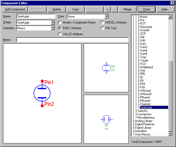
The Component Editor settings for the spark-gap macro appear below. The Name is defined with the same name as the macro circuit. The Sparkgap shape was created in the Shape Editor for this macro. The definition is defined as macro, and two pins are defined for the component. The two pins are Pin1 and Pin2 which are the labels on the nodes across the spark-gap in the macro circuit.
|

|
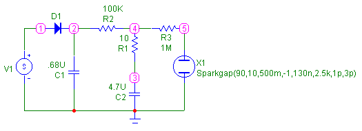
A test circuit for the spark-gap model appears below. This is a simple self-relaxing configuration. The spark-gap macro has its VALUE attribute defined as:
Sparkgap(90,10,500m,-1,130n,2.5k,1p,3p)
whose values correspond to a Siemens A81-C90X arrestor. The input voltage source, V1, has been defined as a sine source with a 320V amplitude at a frequency of 50Hz. The diode is a 1N4007 model.
|

|
The resulting transient analysis appears below. The simulation has been run for 200ms with a Maximum Time Step of 20us. However, the two waveforms have been zoomed in so that it is displaying the waveforms between 177ms and 178ms. This is the time range where the spark-gap reaches its striking voltage. As can be seen in the analysis results, the spark-gap voltage, V(5), has reached the striking voltage of 90V and trips at that point where it falls to its arc voltage value of 10V. The current through the spark-gap, I(R3), spikes up at that point. The spark-gap continues conducting until the current falls below the specified sustaining level of .5A at which point it resumes acting like an open circuit.
|
|
|
|
|


