|
|
 |
Modeling a Commercial Digital Component
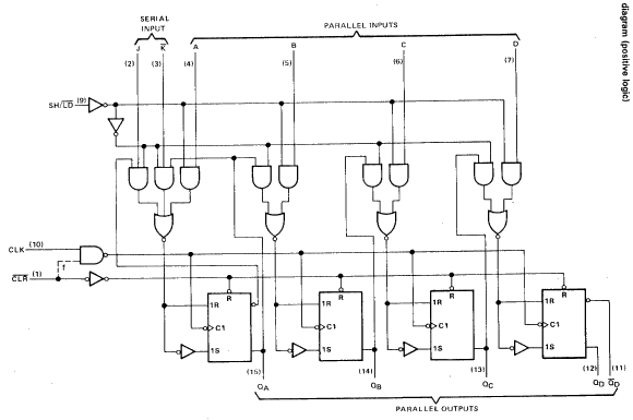
Although Micro-Cap has many digital models, a user may need one that does not exist in the library. In that case, a subcircuit or macro model of the digital component would need to be created. The following article covers the process of creating a digital subcircuit model from data book information. The model that is to be created is the 74195, which is a 4-Bit Parallel-Access Shift Register. Data book information about this component can be viewed in the "TTL Logic Data Book" from Texas Instruments, 1988, p. 2-655 to 2-662. The logic diagram appears below. This register features parallel inputs, parallel outputs, J-K serial inputs, shift/load control, and an overriding clear.
|

|
The subcircuit listing for the 74195 component appears below. This subcircuit is also available in the DIG195.LIB library file that comes with Micro-Cap. The model consists of a subcircuit header, a .Ends statement, and four different devices: a logic expression device, a J-K flip-flop array, a pin-to-pin delay device, and a constraint device. The description of each of these is as follows:
	.SUBCKT 74195  CLK SH/LDBAR J KBAR CLRBAR A B C D QA QB QC QD QDBAR
	+  optional: DPWR=$G_DPWR DGND=$G_DGND
	+  params: MNTYMXDLY=0 IO_LEVEL=0

	U74195 LOGICEXP(13,9) DPWR DGND
	+      CLK SH/LDBAR J KBAR CLRBAR A B C D QA_O QB_O QC_O qabar
	+      j0 j1 j2 j3 k0 k1 k2 k3 clock
	+      D0_GATE IO_STD MNTYMXDLY={MNTYMXDLY} IO_LEVEL={IO_LEVEL}
	+
	+    LOGIC:
	+      clock = {(~(CLK & CLRBAR))}
	+      k0 = {~((SH/LDBAR & J & qabar) | (SH/LDBAR & KBAR & QA_O) |
	+               (~SH/LDBAR & A))}
	+      k1 = {~((QA_O & SH/LDBAR) | (~SH/LDBAR & B))}
	+      k2 = {~((QB_O & SH/LDBAR) | (~SH/LDBAR & C))}
	+      k3 = {~((QC_O & SH/LDBAR) | (~SH/LDBAR & D))}
	+      j0 = {(~k0)}
	+      j1 = {(~k1)}
	+      j2 = {(~k2)}
	+      j3 = {(~k3)}

	Uf0  JKff(4)  DPWR DGND
	+    $D_HI CLRBAR clock
	+    j0 j1 j2 j3 k0 k1 k2 k3
	+    QA_O QB_O QC_O QD_O  qabar qbbar qcbar QDBAR_O
	+    D0_EFF IO_STD MNTYMXDLY={MNTYMXDLY} IO_LEVEL={IO_LEVEL}

	Udly PINDLY (5,0,2) DPWR DGND
	+    QA_O QB_O QC_O QD_O QDBAR_O
	+    CLK CLRBAR
	+    QA QB QC QD QDBAR
	+    IO_STD MNTYMXDLY={MNTYMXDLY} IO_LEVEL={IO_LEVEL}
	+
	+    BOOLEAN:
	+     CLOCK = {CHANGED_LH(CLK,0)}
	+     CLEAR = {CHANGED_HL(CLRBAR,0)}
	+
	+    PINDLY:
	+       QA QB QC QD QDBAR = {
	+            CASE(
	+                 CLEAR, DELAY(-1,19ns,30ns),
	+                 CLOCK & TRN_LH, DELAY(-1,14ns,22ns),
	+                 CLOCK & TRN_HL, DELAY(-1,17ns,26ns),
	+                 DELAY(-1,20ns,31ns)
	+                )
	+            }

	Ucnstr CONSTRAINT(9) DPWR DGND
	+    CLRBAR CLK A B C D J KBAR SH/LDBAR
	+    IO_STD IO_LEVEL={IO_LEVEL}
	+
	+      FREQ:
	+         NODE = CLK
	+         MAXFREQ = 30MEG
	+      WIDTH:
	+         NODE = CLK
	+         MIN_HI = 16ns
	+      WIDTH:
	+         NODE = CLRBAR
	+         MIN_LO = 12ns
	+      SETUP_HOLD:
	+        CLOCK LH = CLK
	+        DATA(6) = A B C D J KBAR
	+        SETUPTIME = 20ns
	+      SETUP_HOLD:
	+        CLOCK LH = CLK
	+        DATA(1) = CLRBAR
	+        SETUPTIME_LO = 25ns
	+      SETUP_HOLD:
	+        CLOCK LH = CLK
	+        DATA(1) = SH/LDBAR
	+        SETUPTIME_LO = 25ns
	+        SETUPTIME_HI = 10ns

	.ENDS 74195
The Subcircuit Header (.SUBCKT)
The subcircuit header denotes the beginning of the subcircuit definition. It defines the node names that are used in calling the subcircuit, along with optional nodes and parameters. All but two of the 74195 's pins have been listed in the subcircuit call. The missing pins are the power and ground pins. These two pins have been placed as optional pins through the "optional:" keyword. Their default values are the globally defined values of $G_DPWR and $G_DGND. Having the power and ground pins as optional pins lets you place the 74195 on a schematic without having to externally connect it to power supplies. The two parameters, MNTYMXDLY and IO_LEVEL, control the digital delay and the digital I/O value, respectively, for the subcircuit and are defined through the "params:" keyword. The default value of 0 specifies that these parameters will take the values of DIGMNTYMX and DIGIOLVL, which are set in the Global Settings.
The Logic Expression Device (U74195)
The logic expression device defines the combinatorial logic that feeds into the flip-flops. This device uses 13 inputs to produce the four J, four K, and one clock input to the J-K flip-flop array. Note that five of the inputs to this device are from the outputs of the flip-flop array. Feedback external to the logic expression is allowed, but feedback in the internal logic expressions is forbidden. The logic expression device is used as a simpler means of defining the logic for a group of gates. The operators available are:
|
| ~ |
Unary negation |
| & |
AND |
| ^ |
Exclusive OR |
| ! |
OR |
| |
By examination, it can be seen that the logic expressions in this device match exactly with the logic in the logic diagram. The k0-k3 outputs correspond to the 1R inputs of the flip-flops, the j0-j3 outputs correspond to the 1S inputs of the flip-flops, and the clock output corresponds to the C1 inputs of the flip-flops. This device has been defined with the D0_GATE timing model, which is a zero delay timing model, and the IO_STD I/O model, which represents the standard TTL family of digital components.
The J-K Flip-Flop Array Device (Uf0)
The JKFF device defines an array of four J-K flip-flops. Though the logic diagram displays S-R flip-flops, the J-K flip-flops can be a direct substitute since the indeterminate state of S=1 and R=1 is logically impossible. The Presetbar pin has been defined as $D_HI, which forces that pin to a high state during simulation so it will have no effect on the flip-flops. The timing model for the array has been defined as D0_EFF which is a zero delay and zero constraint timing model.
The Pin-to-Pin Delay Device (Udly)
The PINDLY device provides a way of modeling conditional pin delays. This device is extremely useful in modeling digital components as all delays may be concentrated in one device, no matter what the trigger of the delay is, instead of having to allocate delays into individual gates in order to produce the correct propagation delays. In this case, the delays for five output pins are being defined with only two reference pins, CLK and CLRBAR. All five outputs share the same propagation delays and therefore, can all be defined in the same case. When an output changes, the pin-to-pin delay device will go through the output's delay conditions and choose the first delay that produces a true result. This could produce an incorrect result if a delay condition after the first true one has the desired propagation delay. Therefore, delay conditions that require a higher precedence should be placed at the top of the list. For example, the 74195 has an overriding clearbar input, so the delay condition that is dependent on the CLRBAR input should be at the top of the list. The -1 value in some of the delay values defines an unspecified setting and the actual delay time will be calculated from the Unspecified Propagation Delay rules. For the 74195, a change in the CLRBAR input from high to low produces a delay of (-1,19ns,30ns). A change in the CLK input from low to high with a corresponding change of low to high in one of the outputs produces a delay of (-1,14ns,22ns). A change in the CLK input from low to high with a corresponding change of high to low in one of the outputs produces a delay of (-1,17ns,26ns). If all of these conditions fail, then the delay of (-1,20ns,31ns) will be used. The delays are specified as (min,typ,max). The specified delays for the 74195 can be found in the Switching Characteristics table in the TI data book.
The Constraint Device (Ucnstr)
The CONSTRAINT device provides a means to check complex conditional timing parameters. It is capable of checking setup time, hold time, pulse width, and frequency specifications. No timing model is required for the device, only an I/O model is needed. The CONSTRAINT device for the 74195 checks the maximum frequency of CLK, the high level pulse width of CLK, the low level pulse width of CLRBAR, and the setup times of all of the inputs in relation to the low to high transition of the CLK input. Any number of FREQ:, WIDTH:, and SETUP_HOLD: keywords may be used. The constraint timing specifications can be found in the Recommended Operating Conditions table in the TI data book. Any violation of these constraints produces a warning, but does not affect the simulation.
The .ENDS Statement
The .ENDS statement signifies the end of the subcircuit. All devices used to model the component must appear between the .SUBCKT and .ENDS statements. The component name that appears on the .ENDS line is optional.
Once the model is finished, the name of the file that contains the model should be placed in the file NOM.LIB if it is not already there. The NOM.LIB file contains a list of all libraries that Micro-Cap accesses automatically. The NOM.LIB file can be found in the DATA subdirectory. If the 74195 was created in a file called 74195.LIB which resides in the DATA directory, then place the following new line in the NOM.LIB file:
.lib "74195.lib"
Adding the 74195 to the Component Menu
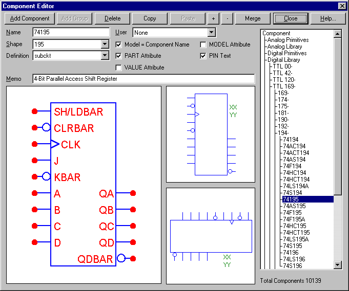
To access the 74195 through the Component menu, the device must be linked to a shape and given pins in the Component Editor. The figure below displays the settings in the Component Editor that were used for the 74195. To add the device, highlight the group that you would like to place it in, and then click on the Add Component command button. This places a new entry into the highlighted group.
The name should be the name that appears on the .SUBCKT line. The shape chosen was the 74195, but it may be any shape that has been created through the Shape Editor. The definition must be 'subckt' to define it as a subcircuit model.
Next, the pins from the subcircuit header need to be entered in the Shape/pin display. Click in the Shape/pin display window at the end of the first lead, and type in the first pin name 'SH/LDBAR'. Click OK. Repeat this process with all of the other pins in the subcircuit header. The pin names must match exactly with the names in the subcircuit header. The pin connection dots and the pin names may each be dragged to their desired location. For easier connections on the schematic, the pin connection dots should be at the end of each lead. The optional power and ground pins could be added in at this point if the part needed to use power supplies available only in the schematic. If the pins are not added, the 74195 will use the power supplies defined in the DIGIO.LIB file. We will leave out the optional pins because their default values are suitable.
Set the checkbox options to how they appear in below. Close and save the component settings. The 74195 component can now be accessed through the Component menu.
|

|
A sample circuit for the 74195 and its resulting analysis appear below. The shift, load, and clear features are all demonstrated in this analysis. As can be seen, the 74195 works as specified according to the function table in the TI data book.
|
|
|
|
|


