|
|
 |
Using the IBIS Components
The IBIS model format was created to model the input and output buffer specifications
of integrated circuits without revealing proprietary information. These models are
widely available from manufacturers and can be used in numerous simulations such as
with transmission line or signal integrity analysis.
A common misconception of many users that we have talked to is that they expect the
IBIS model to simulate the actual device. IBIS models do not model the internal
logic of the device. They only simulate the I/O buffer structure. For simulation
of the actual device, a SPICE model needs to be used instead. The typical IBIS file
contains the current and voltage characteristics, package parasitics, and protection
device characteristics of the I/O buffer structures.
While Micro-Cap contains the IBIS Translator that converts IBIS files into SPICE
libraries, the simpler method to using IBIS models in a schematic is to use the IBIS
components available in the Analog Primitives / IBIS section of the Component menu.
Placing an IBIS component in a schematic invokes the IBIS Model Creator dialog box
which lets a single pin/signal be selected for extraction from a specified IBIS file.
The IBIS component then creates a subcircuit model for either an input or an output
buffer model from the information available within the IBIS source file. This
subcircuit model is created dynamically when the IBIS component is placed in the
schematic, and the subcircuit is stored in the Models text page of the schematic.
There are four IBIS components available in Micro-Cap. The four components along with
their descriptions are:
IBIS_Input1 - Input buffer model with internal power supplies
IBIS_Input3 - Input buffer model with external power supplies
IBIS_Output3 - Output buffer model with internal power supplies
IBIS_Output5 - Output buffer model with external power supplies
For the IBIS_Input1 and the IBIS_Output3 components, the power supplies for the devices
are created within the subcircuits using the supply values specified in the IBIS file.
For the IBIS_Input3 and IBIS_Output5 components, the user has to connect the power pins
on the components to supplies in the schematic.
Using the components
The first step in using an IBIS component is to get the appropriate IBIS file from the
manufacturer of the device. These files are usually available on the company's website
so they are easy to download. For this example, an IBIS file from NXP that contains
IBIS models for the I/O buffers of the 74AHC00 quad 2-input Nand gate will be used.
This IBIS file should be stored in the Library folder of Micro-Cap.
The next step is to enter one of the IBIS components in the schematic. The IBIS_Input3
component is selected from the Analog Primitives / IBIS section and is placed in the
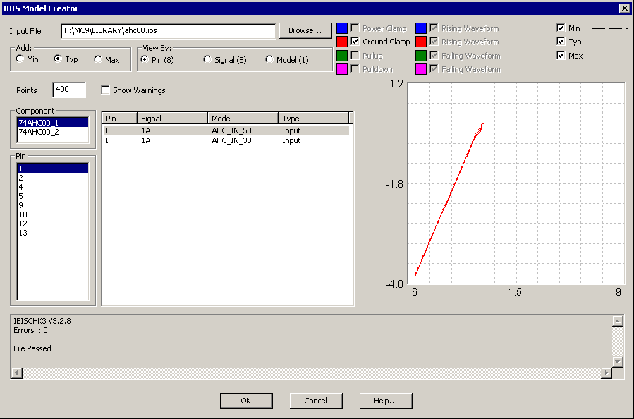
schematic. Upon placement, the IBIS Model Creator dialog box shown in below will appear.
|

|
The IBIS Model Creator dialog box consists of the following items:
Input File: This field specifies the IBIS file name. The file should have an IBIS
extension (IBS). The Browse button can be used to browse the library or other folders
for IBIS input files.
Add: This determines whether the minimum, typical, or maximum values from the IBIS
file are to be used when creating the SPICE model.
View By: This determines whether pin, signal, or model names are displayed in the
Item List.
Points: This determines the number of data points the translator uses in the PWL
tables.
Show Warnings: If the parser issues a warning, this check box determines whether
it will be printed in the Message Box.
Component: This selects one of the component names in the file.
Item List (Pins or Signals or Models): This shows either the pin, signal, or model
names depending upon the View By setting. Selecting one or more of the items in this
list displays them in the IBIS Display.
IBIS Display: This shows all the available IBIS models available for the selected item
in the Item List. This list selects the actual buffer model that will be created.
Plot Controls: The checkboxes in the upper right let you display the specified plots
for the buffer that have been defined within the IBIS file.
Plot Area: This is where the IBIS file plots are displayed.
In the figure above, the Input File field has been set to the AHC00.IBS file from NXP
that is now present in the Library folder. All of the input buffer models within the
AHC00.IBS file are now available to create a subcircuit model for.
There are two components available in this IBIS file: 74AHC00_1 and 74AHC00_2. The
74AHC00_1 models the device with a SO 14-pin package, and the 74AHC00_2 models the
device with a TSSOP 14-pin package. In this case, the 74AHC00_1 is selected.
The View By field has been set to Pin, so all of the input pins for the 74AHC00 device
are shown in the Item List. Selecting pin 1 in the list shows that there are two
available models in the IBIS file for this pin: AHC_IN_50 and AHC_IN_33. The
AHC_IN_50 model is for use with a 5V supply, and the AHC_IN_33 model is for use with
a 3.3V supply.
The descriptions mentioned above for the components and models were found within
comments in the IBIS file. The IBIS file can be viewed within any text editor.
With the AHC_IN_50 model selected for pin 1, clicking the OK button in the IBIS Model
Creator dialog box will then display the standard Attribute dialog box for components.
At this point, the subcircuit model has been created and given the name AHC_IN_50_1_TYP
which combines the model name, the pin name, and whether it is using minimum, typical,
or maximum values. The IBIS button in the Attribute dialog box can be used to invoke
the IBIS Model Creator dialog box again. Clicking OK in the Attribute dialog box will
then add the IBIS component and place the subcircuit into the Models page of the
schematic.
To model an IBIS output buffer, the same procedure is used. In this case, the
IBIS_Output5 component is selected from the Analog Primitives / IBIS section and is
placed in the schematic. With the AHC00.IBS file set as the input file, the IBIS
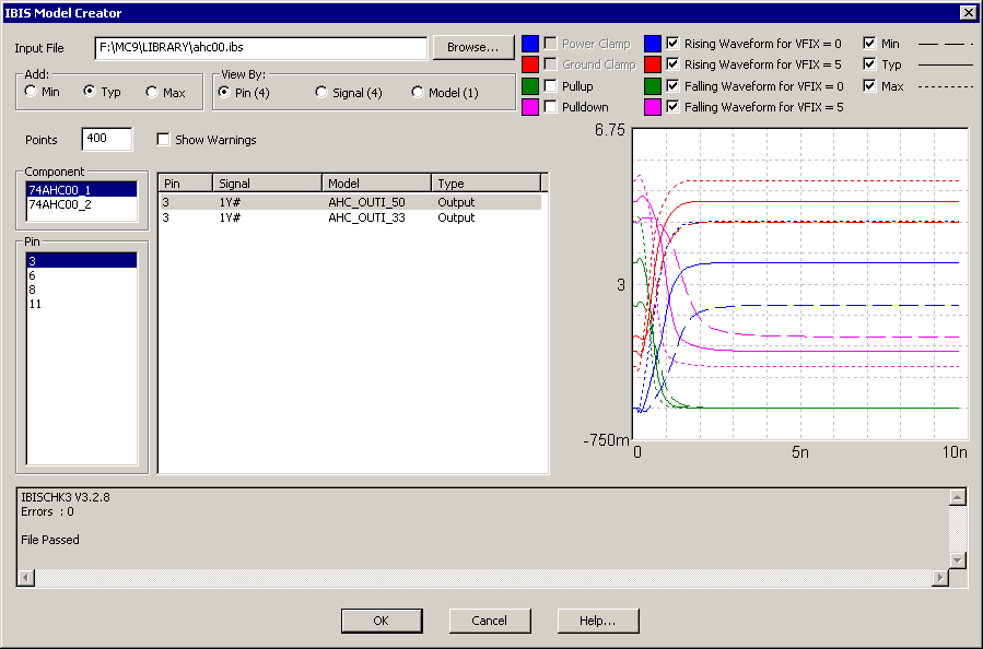
Model Creator dialog box appears as below.
|

|
The View By field has been set to Pin, so all of the output pins for the 74AHC00 device
are shown in the Item List. Selecting pin 3 in the list shows that there are two
available models in the IBIS file for this pin, AHC_OUTI_50 and AHC_OUTI_33, which
respectively model the output buffer with a 5V supply and a 3.3 volt supply.
With the AHC_OUTI_50 model selected for pin 3, clicking the OK button then displays the
Attribute dialog box. The subcircuit created in this instance is called
AHC_OUTI_50_3_TYP. Clicking OK again adds the part and the subcircuit model to the
schematic file.
Example schematic
Using the IBIS input and output buffer models that were created through the above
procedure, a simple circuit has been created to simulate the 74AHC00 I/O
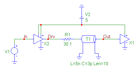
characteristics. The circuit is shown in the figure below.
|

|
The IBIS_Output5 device, X2, models the output buffer of a 74AHC00 component. This
device has five pins. The input pin is tied to a pulse source, V1, that produces a
5V, 40ns pulse that simulates both a rising and falling transition through the output
buffer. The negative power supply is grounded. The positive power supply along with
the enable pin are tied to a 5V battery. The output pin is connected to a 30.1 ohm
resistor which in turn is connected to a transmission line component. The transmission
line has its VALUE attribue defined as:
L=5n C=3p Len=10
This simulates the inductance and capacitance of the signal route between the output
buffer and the input buffer. Finally, the IBIS_Input3 device, X1, models the input
buffer of a 74AHC00 component. This device has three pins. The input pin is
connected to the other side of the transmission line. The negative power supply is
grounded, and the positive power supply is set to 5V. The IBIS input buffer has no
output pin as it is intended to model the load placed on a signal when the buffer is
connected to it.
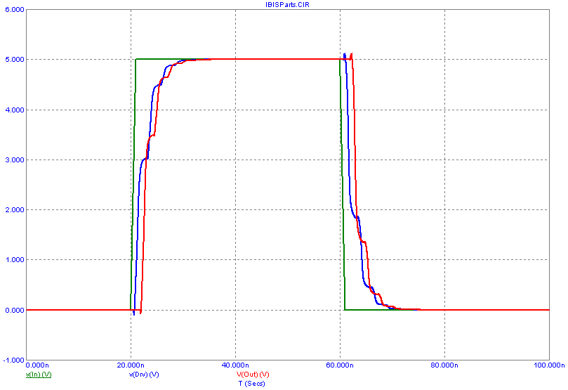
The goal of this simulation is to see how the signal propogates between the output of
a 74AHC00 device and one of the inputs of another 74AHC00 device going through a route
that has the basic characteristics modelled by the resistor and transmission line.
The resulting transient analysis is displayed below. Three waveforms have been
plotted. V(In) plots the pulse signal created by the V1 voltage source. V(Drv) plots
the voltage waveform at the output of the X2 output buffer. V(Out) plots the voltage
waveform at the input of the input buffer.
|

|
|
|
|
|


