|
|
 |
CPFSK Modulator Macro
Frequency modulation can be performed through various frequency shift keying (FSK)
methods. FSK is a way to represent binary information by modifying a sinusoidal
carrier signal between two different frequencies. The mark frequency represents
the binary one state, and the space frequency represents the binary zero state.
One drawback to standard FSK modulation is that at the transition point between the
mark frequency and the space frequency, the phase can be discontinuous. These
discontinuities can produce unwanted nonlinear effects in some circuits. Continuous
phase frequency shift keying (CPFSK) is a variation of FSK which eliminates these
phase discontinuities. CPFSK modulation produces a signal with the following
expression:

where Ac is the amplitude of the CPFSK signal, fc is the base carrier frequency, and Df
controls the frequency deviation. m(t) is the message signal, and integrating this
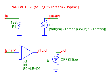
signal provides the continuous phase of the CPFSK. The schematic for a CPFSK modulator
macro appears below.
|

|
The macro circuit has five parameters that are passed through to it: Ac, Fc, Df,
VThresh, and Type. The Ac, Fc, and Df parameters all perform the same functions
as their counterparts in the above CPFSK modulation expression. The VThresh parameter
defines the analog voltage value that will be the threshold voltage in determining
whether the message signal should be considered a binary one or a binary zero. At
or above this threshould, the message signal will be regarded as a binary one. Below
this threshold, the message signal will be regarded as a binary zero. The Type
parameter sets whether the higher CPFSK frequency is assigned to the mark frequency
or the space frequency. If Type=1, the mark frequency is set to the higher frequency.
If Type=2, the space frequency is set to the higher frequency.
The In node is the node where the message signal will be input. The R1 resistor is
present at this input node for two reasons. The first reason is to provide a DC path
to ground for the In node so that any element may be connected to it. The second reason
is that the NFV sources are only able to work with analog references. If the input
waveform happens to be a digital waveform, this resistor will force Micro-Cap to
convert it to its equivalent analog voltage for use with the E2 nonlinear function
voltage source. The value of the resistor is set to 1e9 ohms so that it will not have
a loading effect.
The E2 NFV source converts the message signal into a binary waveform whose analog
voltage levels are at 1 and -1. The E2 source has its VALUE attribute defined with
the following expression:
(V(In)>={VThresh}) - (V(In)<{VThresh})
When the voltage at node In is greater than or equal to the specified VThresh
parameter, the first half of the expression evaluates to true and the output of the
source is 1. When the voltage at node In is less than VThresh, then the second half
of the expression evaluates to true and the output of the source is -1.
The binary waveform is then input into the X1 Int macro which performs the integration
of the message signal that provides the continuous phase performance of the modulator.
The Scale value of the integrator macro has been defined with the Df parameter which
controls the frequency deviation of the CPFSK output.
Finally, the output of the CPFSK modulator is created through the E1 NFV source. The
E1 source has its VALUE attribute set with the variable CPFSKExp. This variable is
defined through the following If statement:
.if Type==2
.define CPFSKExp Ac*cos(2*PI*(Fc*t - V(IntOut)))
.else
.define CPFSKExp Ac*cos(2*PI*(Fc*t + V(IntOut)))
.endif
where V(IntOut) is the voltage output of the Int macro. This source reproduces the
basic CPFSK equation shown at the beginning of the article. Depending on the value
of the Type parameter, one of these CPFSK expressions will be used. The only difference
between the two is whether the IntOut voltage is added or subtracted within the Cos
expression.
A simple test circuit for the CPFSK modulator is shown below. The circuit consists of
a simple two bit shift register that feeds the CPFSK macro. The two D flip-flops are
defined with zero gate delays. The clock input to the flip-flops has a period of 5ms.
The preset inputs have been wired to a Fixed Digital component which produces a constant
one state on those pins. The clear inputs have a short zero state pulse of 100ns to
initialize the Q outputs of the flip-flops to zero at the beginning of the simulation.
The CPFSK macro has its parameters set as the following:
AC = 3
FC = 1700
DF = 400
VTHRESH = 2
TYPE=1
This combination of parameters will produce a 3 volt sinusoidal output whose mark
frequency is at 2100Hz and space frequency is at 1300Hz. The input voltage threshold
is set at 2 volts.
|

|
The analysis plot below shows the results of a 40ms transient simulation. The top
waveform, V(Out), is the input into the modulator. The bottom waveform, V(FSK_Out),
is the modulated output.
The two performance tags in the bottom plot calculate the frequencies of the third
cycle and the fiftieth cycle of the modulated output. The third cycle occurs when
the modulator input is at a zero state and shows the space frequency. The fiftieth
cycle occurs when the modulator input is at a one state and shows the mark frequency.
Both frequencies are calculated at the expected values of 1300Hz and 2100Hz.
|
|
|
|
|


