|
|
 |
Using Global Nodes
Global nodes are nodes whose names are globally available to all levels of the circuit,
from the top level through to any macros or subcircuits used in the circuit. Using a
global node name will tie all nodes together that share the same name whether they are
in the main circuit or in a subcircuit three levels down. This feature provides a
powerful method to assign common characteristics such as power supplies throughout a
multilevel schematic. Global nodes are designated by prefacing the node name with
$G_ in the following format:
$G_Name
In the Micro-Cap libraries, global nodes are used extensively in the modelling of the
digital components to define the circuitry at the power supply pins of each component.
In the digital interface library (DIGIO.LIB), the main power supplies for the digital
families are defined within subcircuits such as:
.subckt DIGIFPWR AGND
+ optional: DPWR=$G_DPWR DGND=$G_DGND
+ params: VOLTAGE=5 REFERENCE=0
V1 DPWR AGND {VOLTAGE}
R1 DPWR AGND 1E9
V2 DGND AGND {REFERENCE}
R2 DGND AGND 1E9
R3 AGND 0 1m
.ends
This subcircuit is used as the power supply for the 74/TTL family of components that
defines the 5 volt power supply and the ground reference for the family. The DPWR and
DGND nodes used within the subcircuit have their default external connections assigned
through the OPTIONAL: statement in the subcircuit header which connects these nodes to
global nodes with the names $G_DPWR and $G_DGND. Each component whose interface model
specifies the DIGIFPWR subcircuit above will also use the $G_DPWR and $G_DGND nodes as
their default power supplies. Consider the 7400 2-input Nand gate model shown below:
.SUBCKT 7400 1A 1B 1Y
+ optional: DPWR=$G_DPWR DGND=$G_DGND
+ params: MNTYMXDLY=0 IO_LEVEL=0
U1 nand(2) DPWR DGND
+ 1A 1B 1Y
+ DLY_00 IO_STD MNTYMXDLY={MNTYMXDLY} IO_LEVEL={IO_LEVEL}
.model DLY_00 ugate (tplhTY=11ns tplhMX=22ns tphlTY=7ns tphlMX=15ns)
.ENDS 7400
The OPTIONAL: statement within the subcircuit header of the 7400 assigns the DPWR and
DGND nodes used within the subcircuit to the same global nodes defined in the power
supply circuit. Note that the U1 nand gate specified in the subcircuit uses the DPWR
and DGND nodes as its power supply references.
Using an On Schematic Power Supply with a Digital Library Part
A Winter 2000 newsletter article described a process by which a digital library component
could access a power supply that exists on the schematic. Using the global node
capability provides a simpler technique for accomplishing the same task.
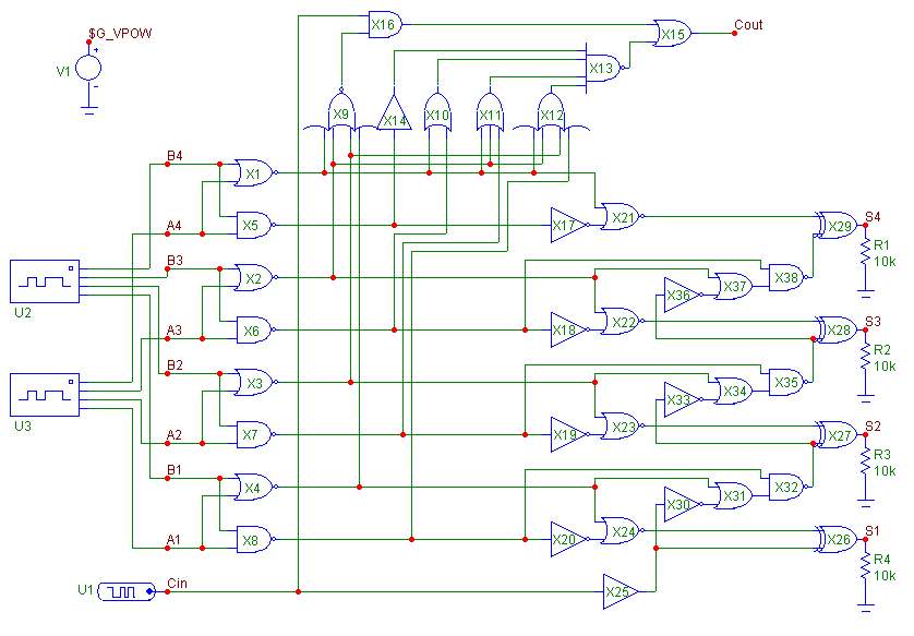
The circuit below simulates a basic 4-bit digital adder. Each of the digital gates in
the adder is taken from the CD4000 family which is capable of handling a wide range of
power supply voltages. In the digital library files, the CD4000 series of parts will
by default access the $G_CD4000_VDD and $G_CD4000_VSS global nodes for their power
supplies as seen in the OPTIONAL: statement within the subcircuit header for the
CD4002B component below:
.SUBCKT CD4002B IN1A IN2A IN3A IN4A OUTA
+ optional: VDD=$G_CD4000_VDD VSS=$G_CD4000_VSS
+ params: MNTYMXDLY=0 IO_LEVEL=0
|

|
To modify these models to use an on schematic power supply, the actual subcircuit header
for the models used in the schematic will need to be edited. Rather than editing the
library file which would affect any other schematic that references the library, the
models can be localized in the schematic file by selecting the Refresh Models command
under the Edit menu. In the Refresh Models dialog box, enable the Subcircuits checkbox
for the Type field as that is the only model type of interest in this circuit. Enable
Add for the Action to use, and then click OK. All of the subcircuits used will now have
their models stored in the Models text page of the schematic. For each of the CD4000
subcircuits, the VDD node is the power supply node. The VDD node assignment in the
OPTIONAL: section of the header will then be assigned to a new global node name such
as:
.SUBCKT CD4002B IN1A IN2A IN3A IN4A OUTA
+ optional: VDD=$G_VPOW VSS=$G_CD4000_VSS
+ params: MNTYMXDLY=0 IO_LEVEL=0
With the above, the VDD node will now be connected to a global node called $G_VPOW. In
the schematic, the power supply for these gates is defined by the V1 pulse source in the
upper left. The pulse source is specified to start at 3V and then rise up to 15V after
2ms at which level it will stay for the rest of the simulation. The node that the
pulse source is connected to has been assigned the global node name, $G_VPOW. The
pulse source will now be connected to the power node of the subcircuit. The VSS node
within the subcircuit will continue to use the ground reference defined within the
DIGIO.LIB file.
The three digital stimulus sources in the schematic have all had their POWER NODE
attribute assigned to the $G_VPOW global node so that they will also use the pulse
source as the power supply. However, since no analog components are connected to the
stimulus sources, the power and ground nodes are never accessed for this simulation by
these sources. The Stim1 source at the Cin input produces a constant 0 output. The
two Stim4 sources at the A and B inputs have had their COMMAND attributes specified to
produce random strings of data. They both use define statements similar to:
.define AIN
+0ns Rnd
+label=start
+.15m ?
+.3m goto start -1 times
where a random Hex state is calculated every 150us. Both the Rnd expression and the
? character can be used to declare a random variable in a digital stimulus
statement.
The 10k resistors at the S outputs of the adder were placed in the schematic so that
the output digital states of the adder would be converted into their equivalent voltage
in order to view the effect that the schematic power supply has on the digital
components. The digital power supplies are only used when an AtoD or DtoA interface is
needed within the schematic.
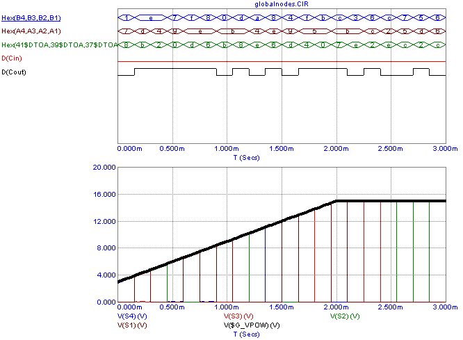
The resulting transient analysis of the adder is displayed below. The top plot displays
the digital states at the inputs and outputs of the adder. The D(Cin) and D(Cout)
waveforms show the binary response for the carry in and carry out nodes of the adder.
The top three waveforms in the plot display the hex results for the A and B input and
the S output states. Note that the hex results for the S outputs reference the internal
digital node names at the outputs with the expression:
Hex(41$DTOA,39$DTOA,37$DTOA,35$DTOA)
The internal digital node names need to be used because with the presence of analog
components at these nodes, any reference to S1, S2, S3, or S4 will assume an analog
voltage which is not applicable with the Hex operator.
The bottom plot shows the analog voltages at the S outputs along with the voltage of the
power supply. The power supply voltage is delineated by the thick black plot. The
CD4000 series of components produce output voltages very close to the power supply rail.
Note how the S outputs rise to whatever the current voltage of the pulse source power
supply is.
|

|
One limitation of the digital/analog interface models in the DIGIO.LIB file is that they
are only specified to work over limited operating voltages. For example, the CD4000
series can operate with power supplies from 3V to 15V. Others, such as the standard
TTL models, are only designed to work at 5V. Operating these components outside of
their range of acceptable power supplies would require the creation of a new I/O model
for the family to produce valid results.
While the example in this article referenced digital circuitry, the use of global nodes
is valid for analog components employing the same technique. This method can be used as
a way to define the power supply of opamps or the common substrate connection of BJTs
through multiple levels of circuitry. Any user who needs a common connection across
multiple levels will find the global nodes a useful tool.
|
|
|
|
|


