|
|
 |
FSK Modulator Macro
In the previous issue of the newsletter, Spring 1998, a PSK modulator macro was introduced that provided a phase modulation technique for superimposing a binary PCM (Pulse-Code Modulation) signal onto a carrier signal. A second modulation technique for this procedure is frequency modulation. Frequency modulation, also known as frequency shift keying (FSK) modulation, produces a waveform with the following characteristics:
VFSK(t) = A * cos((wo + k) * t)
where A is a fixed amplitude, and the frequency will vary according to the binary PCM waveform. For example, if the length of a single bit of the binary PCM waveform is 10us, an FSK modulator may produce a waveform where the frequency is 200KHz when the binary signal is at a zero state and 400KHz when the binary signal is at a one state.
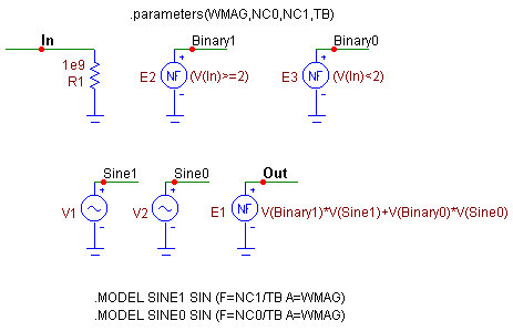
The macro circuit for an FSK modulator appears below. This macro can accept either a digital or an analog waveform as its binary PCM input signal and will produce the corresponding FSK modulated waveform at its output. The FSK macro accepts four parameters: WMAG, NC0, NC1, and TB. WMAG defines the magnitude of the output waveform. NC0 defines the number of cycles of the output waveform that will occur in the duration of a single zero bit of the input waveform. NC1 defines the number of cycles of the output waveform that will occur in the duration of a single one bit of the input waveform. TB defines the duration of a single bit in seconds.
|

|
The macro consists of a resistor, two sine sources, and three nonlinear function voltage sources. The resistor is present at the input node for two reasons. The first reason is to provide a DC path to ground for the In node so that any element may be connected to it. The second reason is that the NFV sources are only able to work with analog references. If the input waveform happens to be a digital waveform, the resistor will force Micro-Cap to convert it to its equivalent analog voltage for use with the nonlinear function voltage sources, E2 and E3. The value of the resistor is set to 1e9 ohms so that it will not have a loading effect. The NFV source, E2, has its VALUE attribute defined as:
(V(In) >= 2)
This equation will convert the input waveform into a signal that has a value of either 1V or 0V. If the voltage at node In is greater than or equal to 2V, than the source will produce an output of 1V, if it is less than 2V, then the output of the source will be 0V. The 2V threshold is arbitrary. In this case, it was setup to handle a standard TTL digital waveform. The threshold should be approximately in the middle of the one and zero state voltages of the input waveform. The NFV source, E3, has its VALUE attribute defined as:
(V(In) < 2)
This source acts in the same manner as the E2 source. However, this source will produce a 1V output whenever the input signal is less than 2V and a 0V output whenever the input signal is greater than or equal to 2V. These two NFV sources will produce a pair of inverted pulse waveforms that correspond to the input PCM signal.
The two sine sources, V1 and V2, have been defined using the following model statements:
.MODEL SINE1 SIN (F=NC1/TB A=WMAG)
.MODEL SINE0 SIN (F=NC0/TB A=WMAG)
The V1 source, with the SINE1 model statement, models the output waveform when the input signal is at a one state. The V2 source, with the SINE0 model statement, models the output waveform when the input signal is at a zero state. The amplitude of each source is defined by the parameter WMAG. The frequency of the sources are determined by the ratios of the NC1 and NC0 parameters to the TB parameter. NC1/TB determines the frequency of the modulated waveform at the one state of the input PCM signal, and NC0/TB determines the frequency of the modulated waveform at the zero state of the input PCM signal.
The NFV source, E1, produces the modulated output waveform from a combination of the four other sources. Its VALUE attribute is defined as:
V(Binary1)*V(Sine1)+V(Binary0)*V(Sine0)
The E1 source takes the product of the voltages at nodes Binary1 and Sine1 and the product of the voltages at nodes Binary0 and Sine0 and sums them together. Since the voltage at either Binary1 or Binary0 must be zero at any given time, the E1 actually alternates between the two sine source voltages depending on the input waveform. If the input signal is greater or equal to 2V, then the output will be the voltage at Sine1, and if the input signal is less than 2V, the output will be the voltage at Sine0.
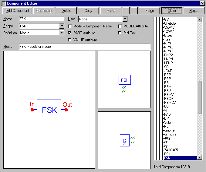
The figure below displays the Component Editor settings for the FSK macro. The FSK shape was created in the Shape Editor, and the component has been defined as Macro. The two pins are named In and Out which correspond exactly to the node names in the FSK macro circuit.
|

|
The test circuit for the FSK macro is displayed below. The circuit consists of a simple two bit shift register that feeds the FSK macro. The two D flip-flops are defined with zero gate delays. The clock input to the flip-flops has a period of 10us. The preset inputs have been wired to a Fixed Digital component which produces a constant one state on those pins. The clear inputs have a short zero state pulse of 100ns to initialize the Q outputs of the flip-flops to zero at the beginning of the simulation. The FSK macro has its VALUE attribute defined as:
FSK(3,2,4,10u)
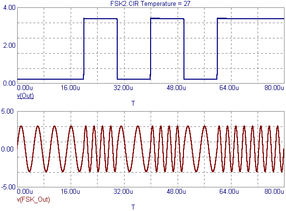
This will produce an FSK modulated waveform with a magnitude of 3V. The frequency when the binary input signal is at a zero state will be 200KHz, and the frequency when the binary input signal is at a one state will be 400KHz.
The plot below displays the results of an 80us transient analysis simulation. The top waveform, V(Out), is the binary input to the FSK macro. The bottom waveform, V(FSK_Out), is the modulated waveform. Note the change in frequencies when the input is at a zero or one state. As can be seen in the figure, the modulated waveform produces two cycles for a single zero bit and four cycles for a single one bit.
|

|

|
|
|
|
|


