|
|
 |
Plotting Y Parameters
Y parameters or short-circuit admittance parameters are useful in the analysis of high frequency components. RF transistors, for example, are usually characterized by Y parameters. The following method extracts the Y parameters from a MRF9411 high frequency transistor from Motorola. This technique was derived from the article "Spice accepts and displays Y parameters" by Michael A. Wyatt which appears in the June 22, 1995 Design Ideas Supplement for EDN.
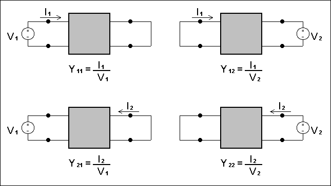
The Y parameters are based on exciting a two port network at one of its ports. The four admittance parameters are defined as follows.
I1 = Y11 * V1 + Y12 * V2
I2 = Y21 * V1 + Y22 * V2
Y11 = I1 / V1 |V2=0
Y12 = I1 / V2 |V1=0
Y21 = I2 / V1 |V2=0
Y22 = I2 / V2 |V1=0
Y11 is the input admittance at port 1 with port 2 short-circuited. Y12 represents the transmission from port 2 to port 1 with port 1 short-circuited. Y21 represents the transmission from port 1 to port 2 with port 2 short-circuited. Y22 is the admittance looking into port 2 with port 1 short-circuited.
The method for measuring each individual parameter would be to short one of the ports while exciting the other. The figure below displays the definition and method for measuring each of these parameters.
|
|
In order to plot the Y parameters versus frequency, an AC analysis needs to be run. The AC analysis is a small signal analysis. It initially calculates a DC operating point and then linearizes the devices about the operating point values. The trick to extracting Y parameters is to be able to bias the circuit correctly while still shorting one of the ports.
|
|
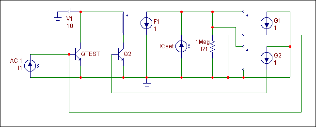
The circuit in the figure above will calculate the Y11 and Y21 parameters for the transistor QTEST, which is a MRF9411 high frequency transistor from Motorola. Q2 is also a MRF9411 transistor and is used to help bias QTEST.
V1, Q2, ICset, F1, R1, G1, and G2 are all used to bias QTEST during the DC operating point operation. The battery V1 supplies the DC supply voltage. During small signal analysis, the battery will act as a short circuit thus providing the circuit with the necessary short at port 2. Q2 is an image device which is identical to the QTEST transistor. ICset, F1, and R1 force the collector current for the two transistors to be equal to the current through ICset. ICset is defined as the value of the collector current that QTEST should be biased at. The current controlled current source, F1, samples the collector current of the Q2 transistor. The value of resistor R1 determines the accuracy of the collector current in relation to the ICset source. The larger the resistor, the closer the collector current will be to the ICset value. The collector current may be calculated through the following equation.
Ic = ICset / (1 + 1/(B*R1))
where B is the beta of the Q2 transistor. With a 1Meg R1 resistor, Ic and ICset are essentially equal. The voltage controlled current sources, G1 and G2, sample the voltage across R1 and produce a base current for each transistor. The base currents will be the same, which forces the collector currents in both transistors to be the same, so that QTEST has been biased with the current set by ICset.
During the small signal analysis, the F1, ICset, G1, and G2 current sources all act as open circuits so the DC bias point circuitry will have no effect. The only source that has been defined with an AC attribute is the current source I1. This source will provide a 1 Amp AC small signal source, exciting port 1, which in this case is the base of QTEST. Note that I1 has no DC component. This causes I1 to act as an open circuit during the DC bias point operation.
|
|
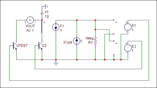
The circuit above will extract the Y12 and Y22 parameters. This circuit operates in a similar manner to the previous circuit. V1, Q2, F1, ICset, and R1 again set the DC bias point for the QTEST transistor, and will have no effect during the small signal analysis. The voltage controlled voltage sources, E1 and E2, are used to bias the base of the transistors. Voltage sources were used in this case instead of the current sources of the previous circuit because the voltage sources will act as the necessary short circuit for port 1 during the small signal analysis. The only source with an AC attribute is the voltage source, Vout. This source provides a 1 Volt AC small signal source that excites port 2. Vout has no DC specification so that it will act as a short circuit during the DC bias point calculation.
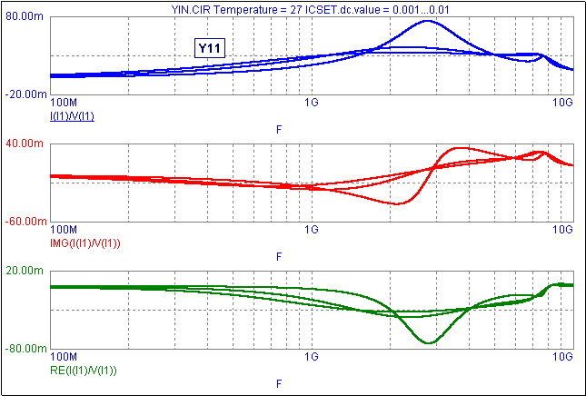
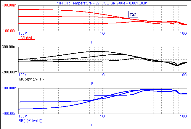
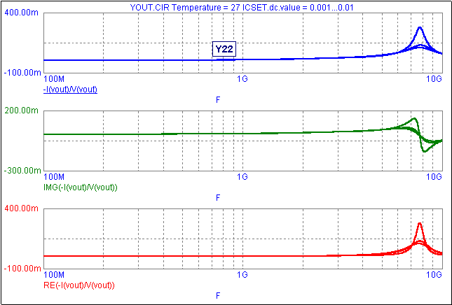
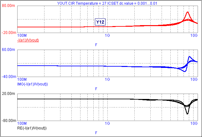
The figures below display the results of these two circuits. Each of the figures displays one of the Y parameters along with its real and imaginary components. Note that in AC analysis, any complex value will automatically have its magnitude plotted, so the negative signs in the equations only have an effect when used in conjunction with the real and imaginary operators. In each of the runs, the ICset source has had its current stepped through the values of 1m, 5m, and 10m using the List option in the Stepping dialog box.
|
|
|
|
|
|
|
|
|


