|
|
 |
Simulating TDR Measurements
Time domain reflectometry (TDR) is a method by which a short duration pulse with a very fast rise time is injected into an
electrical line in order to solve signal integrity issues. The reflected waveform from this pulse can be used to calculate
the characteristics of the line such as the impedances and propagation delays along the signal path. This measurement can
give a good indication of any discontinuites within the line that would occur with an open, short, or any other impedance
mismatch.
Both of the examples used in this article were derived from the Maxim application note shown in Reference 1. The schematic
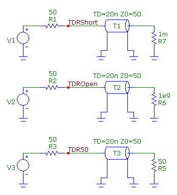
shown below is used to demonstrate the basics of a TDR measurement. There are three separate circuits in the schematic.
The only difference between the three is the value of the load resistance. The top circuit models a short at the line
output. The middle circuit models an open at the line output. The bottom circuit models the case where the load impedance
matches with the line impedance. A voltage source at the input to each of the circuits injects the fast rising pulse
necessary to make the TDR measurement. Each of the voltage sources has its VALUE attribute defined as:
Pulse 0 2 0 25p 10n 1 4
This definition creates a 2 volt rising edge waveform with a rise time of 25ps. The width and period of the pulse are set to
values high enough so that the falling edge of the pulse is not simulated. The source resistance in each circuit has been set
at 50 ohms. The electrical line is modelled by a transmission line component whose VALUE attribute is:
TD=20n Z0=50
This creates an ideal transmission line that has a time delay of 20ns and a characteristic impedance of 50 ohms.
|

|
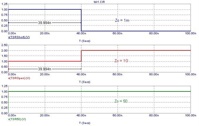
The TDR measurement is run within a transient analysis. The simulation of the TDR measurements for each of the three circuits
is displayed in the plots below. The simulation has been run for 100ns. The waveforms plotted are the voltages between the
source resistances and the transmission line inputs. Since the time delay of the transmission line has been specified as
20ns, the reflected waveforms will appear after 40ns since the signal has to travel through the transmission line and back.
|

|
The top plot shows the TDR for the short circuit load. For a short circuit load, the reflected waveform is equal to the
incident waveform but opposite in polarity so that the incident waveform is cancelled when the reflected waveform has propagated
back through the transmission line at 40ns.
The middle plot shows the TDR for the open circuit load. For an open circuit load, the reflected waveform is equal to the incident
waveform and has the same polarity so that the incident waveform is reinforced when the reflected waveform has propagated back through
the transmission line at 40ns.
The bottom plot shows the TDR for the matched load. For a matched load, there is no reflected waveform, and the incident waveform is left intact.
The amplitude of the reflected waveforms can be used to calculate the impedances of the loads. The load impedance can be calculated
from the following expression:
ZL = ZO * (1 + ρ) / (1 - ρ)
where ZL is the load impedance, ZO is the characteristic impedance and ρ is the reflection coefficient of the signal. This expression can
be calculated within the analysis plot using the Formula capability of the analysis text. The following analysis text calculates the load
impedance in each of the plots. The formula delimiters have been set as the square brackets, [ ].
Zo = [50*(1+(Y_Level(v(TDR50),1,1,50n)-1))/(1-(Y_Level(v(TDR50),1,1,50n)-1))]
The reflection coefficient is calculated by dividing the magnitude of the reflected waveform by the incident waveform. Since the incident waveform
has a value of 1V in this example, the reflection coefficient can be calculated by measuring the magnitude of the waveform at a specific time and
subtracting the incident waveform value to get the magnitude of the reflected waveform. The reflection coefficient is calculated in the above
expression through the term:
Y_Level(v(TDR50),1,1,50n)-1
The Y_Level function returns the value of the voltage at node TDR50 at a time of 50ns. Subtracting one, which is the magnitude of the incident
waveform, returns the magnitude of the reflected waveform. The formula analysis text in each plot correctly displays the value of the corresponding
load resistor in the schematic.
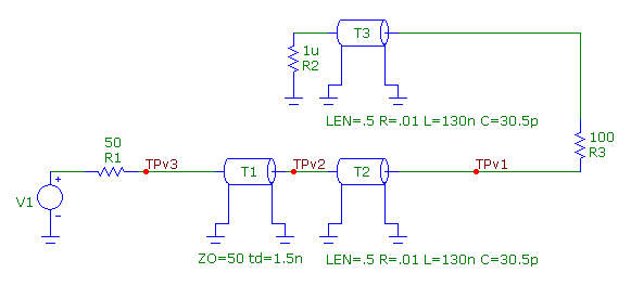
The second example models the delay from an SMA edge connector to the DATA1 and NDATA1 input pins of a MAX9979 IC. The schematic is shown below.
The V1 voltage source models the TDR input signal, and the R1 resistor is the TDR source resistance. The T1 transmission line models the test cable
and has its VALUE attribute defined as:
ZO=50 td=1.5n
This gives the line a characteristic impedance of 50 ohms and a time delay of 1.5ns. The T2 and T3 lossy transmission lines model the PCB traces to the
DATA1 and NDATA1 pins. Both of these traces are symmetrical and have identical lengths so the VALUE attribute for both transmission line components have
been defined as:
LEN=.5 R=.01 L=130n C=30.5p
These values produce lines with a characteristic impedance of 65 ohms and a delay of approximately 1ns.
|

|
There is a 100 ohm resistor that goes between these two pins which is represented by R3. For this example, the NDATA1 pin has been terminated to ground.
The resulting transient analysis is shown below. The first reflected waveform occurs at 3ns which is twice the time delay of the test cable. Using
the formula text described previously on this reflection calculates the impedance at approximately 65 ohms which matches the impedance of the T2
transmission line. This reflection lasts for 2ns which confirms the time delay of 1ns for the line. Secondary reflections occur at the test point as
the signal settles down. The impedance calculation at the end of the simulation shows the 100 ohms from the R3 resistor.
|
Reference:
1) "Propagation Delay Measurements Using TDR", http://www.maxim-ic.com/app-notes/index.mvp/id/4395, Bernard Hyland, Maxim Application Note 4395
|
|
|
|
|


