|
|
 |
Modeling Switch Bounce
Switch bounce, also referred to as contact bounce, is a common issue with many types of mechanical switches.
Ideally, when the switching contact strikes another contact, it would immediately stick to that contact.
However, due to the contact's momentum and elasticity, the switching contact can bounce a few times before
coming to rest. This produces a pulse like effect as the switch rapidly opens and closes.
The standard switch models in Micro-Cap do not model switch bounce. These switches all have an ideal transition
where they open or close cleanly. In order to model switch bounce, additional circuitry needs to be added to the
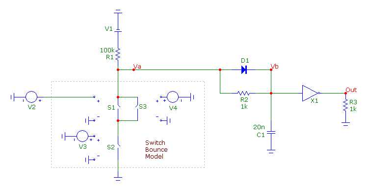
switch. The schematic below displays one method of simulating switch bounce.
|

|
The switch bounce model is contained within the dashed rectangle in the schematic. It consists of three S
(V-Switch) components and two voltage source components. The S1 switch is the main switch. The inputs to this
switch control whether the switch model will be opened or closed. This switch is defined with the following
model:
.MODEL MAIN VSWITCH (ROFF={2*Roff} RON={Ron/2} VOFF={Voff} VON={Von})
All of the parameters are defined through the symbolic variables Roff, Ron, Voff, and Von. These four
symbolic variables are set through the following define statements.
.Define Von 2.5
.Define Voff 2
.Define Ron 1m
.Define Roff 10Meg
The Von and Voff variables directly define the on and off voltages of the switch. In this case, the switch
will close when the input voltage is greater than 2.5V and open when the input voltage is less than 2V. In between
these two input values, the switch will smoothly transition between the on and off resistances. The Ron and
Roff variables define the on and off resistances of the switch bounce model and need to be scaled within the
switch model statement to account for the other switch resistances in the circuit.
The S2 switch and the V3 voltage source model the switch bounce when the main switch closes. The S2 switch
is defined with the following model:
.MODEL BOUNCE VSWITCH (ROFF={Roff} RON={Ron/2} VOFF=3 VON=2)
Both of the S1 and S2 switches need to be closed for the entire switch bounce model to be closed. Due to this,
each of these switches needs to model half of the on resistance since they are in series. Therefore, both of
these switch models have their on resistance defined as Ron/2. When the V3 voltage source at the input to the
switch is below 2V, the switch is closed and when it is above 3V, the switch is open. The V3 source has its
VALUE attribute set to:
PWL TRIGGER={(R(S1) < Ravg)} 0,0 .999m,0 1m,5 2m,5 2.001m,0 2.499m,0 2.5m,5 3m,5 3.001m,0 3.3m,0 3.301m,5 3.5m,5 3.501m,0
The voltage source has a piecewise linear definition. The source is dormant until the TRIGGER expression evaluates
to true. To trigger this source, the resistance of the S1 switch must fall below the value of the variable Ravg
where Ravg is set through the following define statement:
.Define Ravg (Roff+Ron)/2
Ravg is the average of the on and off resistances of the switch bounce model. When the resistance of S1 falls
below this value, that indicates that the switch has closed. At that point, the V3 source will output the specified
PWL waveform. In this case, the PWL waveform will cause the S2 switch to open and close three times over the course
of the next 3.5ms which simulates the switch contact bouncing.
The S3 switch and the V4 voltage source model the switch bounce when the main switch opens. It works in a
similar manner to the S2 and V3 combination. The S3 switch model is defined as:
.MODEL BOUNCE2 VSWITCH (ROFF={2*Roff} RON={Ron/2} VOFF=2 VON=3)
Both of the S1 and S3 switches need to be open for the entire switch bounce model to be open. Due to this, each of
these switches needs its off resistance set to 2*Roff since they are in parallel. In addition, the on resistance of
S3 also needs to be set to Ron/2 since it will be in series with the S2 switch when it is closed. The V4 voltage
source is connected to the input of S3 and has its VALUE attribute defined as:
PWL TRIGGER={(R(S1) > Ravg)} 0,0 .999m,0 1m,5 2m,5 2.001m,0 2.499m,0 2.5m,5 3m,5 3.001m,0 3.3m,0 3.301m,5 3.5m,5 3.501m,0
To trigger this source, the resistance of the S1 switch must rise above the Ravg value. When the resistance of S1 rises
above this value, that indicates that the switch has opened. The resulting PWL output will cause the S3 switch to close
and open three times over the course of the next 3.5ms which simulates the switch contact bouncing upon opening.
This model can be easily modified. The PWL waveforms can be changed to model the appropriate switch bounce characteristics.
The PWL waveform values chosen in this example were completely arbitrary. If the bounce needs to be simulated only upon
either an open or close, the S2 or S3 switch can be deleted from the model. Note that the on and off resistances of the
remaining switches may need to be adjusted if either the S2 or the S3 switch is deleted.
In this example circuit, the switch bounce model is connected to a 100Kohm resistor which goes to a 5V battery. The Va node
at the junction of the switch and resistor is fed into a simple debouncing circuit consisting of a diode, resistor, capacitor,
and inverter. The resistor and capacitor mitigate the switch bounce transitions enough so that they have no effect on the
inverter. The inverter then restores the sharp transitions of the switch.
The debouncing circuit portion of the circuit is first disabled. This is done by drawing a select box around the debouncing
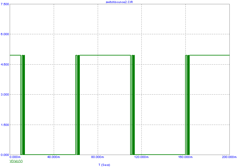
circuitry and then choosing Disable from the Edit menu. Running transient analysis produces the simulation plot below.
|

|
The V(Va) waveform clearly shows the pulse like effect produced by the switching contact bouncing upon both the open and close
transitions. The bouncing transitions match precisely with the PWL waveforms that were defined within the switch bounce model.
The debouncing circuit is then enabled again by drawing a select box around the debouncing circuitry and then choosing the Enable
command under the Edit menu. Running the transient analysis produces the simulation plot below. The voltage waveform produced by
the bouncing has been greatly minimized as shown in the plots for V(Va) and V(Vb). The V(Out) waveform shows that the inverter has
produced the sharp, clean transition edges that one would want from the switch.
|
|
|
|
|


