|
|
 |
HSPICE Style MOSFET Binning
MOSFET binning is the process of adjusting model parameters for different values of drawn
channel length and width. While the original Berkeley method of binning is available for
all BSIM models, the HSPICE binning is only available for BSIM3 and BSIM4 models.
HSPICE style binning uses multiple model statements to model the MOSFET characteristics
over a range of lengths and widths. Each model statement models a portion of the length
and width ranges. There are eight MOSFET parameters that apply to HSPICE style binning.
They are as follows:
LMIN - This parameter defines the minimum length that the model statement will apply to.
LMAX - This parameter defines the maximum length that the model statement will apply to.
WMIN - This parameter defines the minimum width that the model statement will apply to.
WMAX - This parameter defines the maximum width that the model statement will apply to.
LREF - This is the reference length that the model parameters are assumed to apply for.
WREF - This is the reference width that the model parameters are assumed to apply for.
BINFLAG - If this parameter is set greater than 0.9 and an LREF or WREF parameter is
present in the model statement, then HSPICE style binning will be available for this
model.
BINUNIT - If this parameter is set to 1, then all geometry parameters are defined in
microns. For any other values, the dimensions are meters.
The LREF and WREF parameters are offset values used to interpolate a value within the
boundaries created by the minimum and maximum length and width parameters. The model
parameters are assumed to apply for the case Leff=LREF and Weff=WREF.
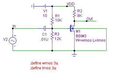
The circuit below provides a simple example of a MOSFET using HSPICE style binning.
|

|
In the text area of this circuit, there are three model statements as follows:
.MODEL BSIM3.1 NMOS (LEVEL=8 LMIN=1U LMAX=5U WMIN=1U WMAX=5U
+ LREF=3U WREF=3U BINFLAG=1 BINUNIT=0 VTH0=0.7 ...)
.MODEL BSIM3.2 NMOS (LEVEL=8 LMIN=5U LMAX=20U WMIN=5U WMAX=20U
+ LREF=15U WREF=15U BINFLAG=1 BINUNIT=0 VTH0=0.9 ...)
.MODEL BSIM3.3 NMOS (LEVEL=8 LMIN=20U LMAX=40U WMIN=10U WMAX=40U
+ LREF=110U WREF=125U BINFLAG=1 BINUNIT=0 VTH0=1.1 ...)
Here BSIM3 is the basic model name and BSIM3.1, BSIM3.2, and BSIM3.3 are the individual
binning models for the width and length values that fall between WMIN and WMAX and LMIN
and LMAX. For HSPICE binning, the model names must have the format NAME.n where NAME is
the model name and n is the number that specifies the individual binning model. Only n
will vary between binning models. The LEVEL=8 parameter declaration defines these MOSFET
models as using the BSIM3 level. Along with the binning parameters shown above, the VTH0
parameter has also been changed between each model in order to demonstrate the use of
binning in the analysis.
The VALUE attribute of the MOSFET has been defined as:
W=wmos L=lmos
with the following define statements in the schematic:
.define lmos 3u
.define wmos 3u
For HSPICE style binning, the length and width must be specified in the VALUE attribute.
Micro-Cap allows L and W to be specified in the model statement, but binning will always
use the length and width specified in the VALUE attribute. In the schematic, the MODEL
attribute of the MOSFET has been defined with the name BSIM3. Since the length and width
were specified in the VALUE attribute, Micro-Cap is going to look for any possible binning
models in the format BSIM3.n that match the length and width specified. If it doesn't
find an appropriate binning model, Micro-Cap will then look for a model that has the name
BSIM3 only. If neither of these searches are successful, an error will be returned.
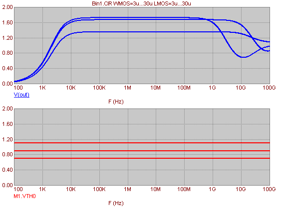
For this example, an AC analysis will be run. The Stepping dialog box has been setup to
step both of the define variables, wmos and lmos, simultaneously. Each of these variables
is defined to step with the List method through the values: 3u, 10u, and 30u. The figure
below displays the resulting AC analysis.
|

|
The simulation produced three runs where the length and width of the MOSFET have been
defined as:
Run1: L=3u and W=3u
Run2: L=10u and W=10u
Run3: L=30u and W=30u
The MOSFET model chosen by Micro-Cap for each run is determined by the width and length
boundaries of the binning models as follows:
WMIN <= W And W <= WMAX
LMIN <= L And L <= LMAX
For each run the following models were used:
Run1: BSIM3.1
Run2: BSIM3.2
Run3: BSIM3.3
In the top plot, the output of the schematic has been plotted. The bottom plot is
displaying the waveform for M1.VTH0. This prints out the value of the model parameter
VTH0 that the MOSFET called M1 in the schematic is using during the run. Note that the
value of VTH0 has changed as expected as a new model is found for each run.
|
|
|
|
|


