|
|
 |
Smooth Transition Time Switch
The Switch component in Micro-Cap has a time dependent method that defines a time window
during which the switch can be on or off. The transition times between the on and off
resistance values of the switch are instantaneous. These instantaneous transitions can
occasionally cause problems with simulation convergence depending on the configuration of
the circuit such as when a switch is in series with an inductor. One method to improve
the convergence is to create a time switch equivalent using the S (V-Switch) component in
conjunction with a nonlinear function voltage source. An example of this equivalent switch
is used in the circuit below.
|

|
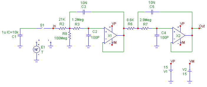
The smooth transition time switch is modeled through the S1 and E1 components in the
schematic. The S1 component is a S (V-Switch) voltage switch. The MODEL attribute
is defined as TIME1 with a corresponding model statement in the text area of:
.MODEL TIME1 VSWITCH (ROFF=1G RON=1m VON=1m VOFF=.95m)
When the input voltage to the switch is less than .95mV, the switch will be off and at a
resistance of 1G. When the input voltage source is greater than 1mV, the switch will be
on and at a resistance of 1m. Between .95mV and 1mV, the resistance is transitioning
between its off and on values. In this range, the switch uses an exponential function
to detemine its resistance. This function provides a smooth resistive transition between
the on and off values which provides a more robust convergence technique. The E1 source
is an NFV function source that has its VALUE attribute defined as T. During transient
analysis, this source will produce a voltage that is equivalent to the current time
being simulated. Since the E1 source is used as the voltage input to the switch, the
combination of the two components mimic a time switch.
In this schematic, the input of the circuit is a 1uF capacitor that has been initially
charged with 10kV across it. The switch is used in series with the capacitor to
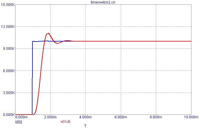
simulate a 10kV pulse. At 1ms, the switch has been turned on to let the voltage pass
through to the low-pass Butterworth filter that follows it. The resulting step response
analysis is displayed below. The two waveforms plotted are the input and output of the
low-pass filter.
|

|
A nice feature of the Switch component is that it is easy to create a window of time
where the switch may be defined as either on or off. The S (V-Switch) and NFV component
combination only models one of these transitions. In order to create a switch that
can produce the equivalent of the time window, two S (V-Switch) components must be used.
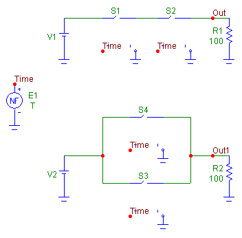
The schematic below shows the two possible orientations that can be created to
model the time window equivalent. The top circuit has two of the switches in series
that use the two following model statements:
.MODEL TIME1 VSWITCH (ROFF=1G RON=1m VON=1m VOFF=.95m)
.MODEL TIME2 VSWITCH (ROFF=1G RON=1m VON=5m VOFF=5.05m)
Both switches must be on for the voltage to pass through them. The combination of the two
switches produces a time window between 1ms and 5ms where the equivalent switch will
be on. Below .95ms and above 5.05ms, one of the two switches will be off, so the equivalent
switch will be off during those times. The bottom circuit has two of the switches in
parallel that use the two following model statements:
.MODEL TIME3 VSWITCH (ROFF=1G RON=1m VON=.95m VOFF=1m)
.MODEL TIME4 VSWITCH (ROFF=1G RON=1m VON=5m VOFF=4.95m)
Either of the switches can be on in order to let the voltage pass through them. The
combination of these two switches produces a time window between 1ms and 5ms where the
equivalent switch will be off. Below .95ms and above 5ms, one of the two switches will
be on, so the equivalent switch will be on during those times.
|

|
The input to all four of these switches is the E1 source at the top which has been
defined as T to represent the simulation time. Only one source is needed for any
number of the S (V-Switch) components since the time input to all the switches is an
independent variable.
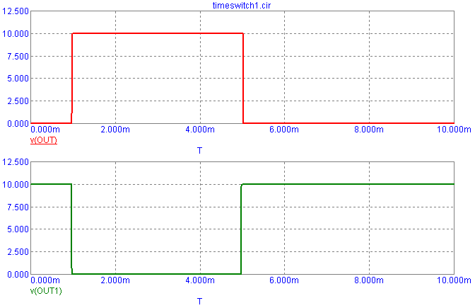
Each of these configurations has a 10V battery at its input and is followed by a 100
ohm resistive load. The analysis of these two configurations is displayed in the plot
below. The top plot is the waveform at the resistive load for the series combination
of switches. The battery voltage has been passed through to the resistor between 1ms
and 5ms where the time window equivalent switch has been defined as on.
The bottom plot is the waveform at the resistive load for the parallel combination of
switches. Note that the voltage is now zero during the time window between 1ms and
5ms since that is the time range that has been modeled as the off state.
This technique provides a good way of overcoming convergence problems when a time switch
is present in a schematic and should be one of the first methods used in trying to
overcome any convergence errors that occur during a time switch transition.
|

|
|
|
|
|


