|
|
 |
Chebyshev Filter Macro
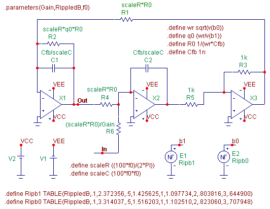
Filters are a circuit element that seem to mesh perfectly with the macro capability of Micro-Cap. The macro capability is designed to produce components that can be varied through the use of parameters. Most filters consist of a basic structure whose component values can be modified through the use of well known equations. A macro component can be created that represents a specific filter's type, order, response, and implementation. The circuit below is the macro circuit for a low pass, 2nd order, Chebyshev filter with Tow-Thomas implementation.
|

|
The macro circuit uses three passed parameters to define the filter. These parameters are Gain, RippledB, and f0. The Gain parameter defines the magnitude of the gain of the filter in the passband region. The RippledB parameter defines the magnitude of the ripple in dB units in the passband region. The f0 parameter defines the cutoff frequency where the filter transitions between the passband and the stopband.
The equations for this macro were taken from Sedra and Smith's "Microelectronic Circuits" book. The Cfb value along with the resistance values for the R3 and R5 resistors are arbitrary. The equations taken from the book are as follows:
wr = sqrt(b0)
q0 = wr / b1
R0 = 1 / (wr * Cfb)
R1 = R0
R2 = q0 * R0
R4 = R0
R6 = R0 / Gain
C1 = C2 = Cfb
The scaleR and scaleC equations are used to scale the resistors and capacitors so that the filter's response occurs at the correct cutoff frequency. The scaleR factor multiplies the value of the R1, R2, R4, and R6 resistors, and the scaleC factor divides the value of the C1 and C2 capacitors.
The three opamps are defined as level 1 opamps and use all default model parameters. These opamps are ideal and will not have an affect on the expected response of the filter. The opamps are powered by +/- 15V batteries although with a level 1 opamp, the battery values will not have an effect.
In the equations for wr and q0, b1 and b0 parameters are specified. The values for b1 and b0 can be found in tables that specify the denominator polynomials for Chebyshev filters. The basic transfer function of the filter is:
1/(s*s + b1 * s + b0)
For this macro, the b1 and b0 values have been defined for when the ripple magnitude is .1dB, .5dB, 1dB, 2dB, and 3dB. These values have been implemented in the following two .define statements.
.define Ripb1 TABLE(RippledB,.1,2.372356,.5,1.425625,1,1.097734,2,.803816,3,.644900)
.define Ripb0 TABLE(RippledB,.1,3.314037,.5,1.516203,1,1.102510,2,.823060,3,.707948)
These two .define statements use the Table operator. The Table operator uses the format:
Table(x,x1,y1,...xn,yn)
where x is the input value and x1,y1,...xn,yn are the data pairs. In this case, the RippledB parameter will be passed into these .define statements. The output of the operator will be the b1 and b0 values that correspond to the RippledB input value. Values entered for RippledB that are not one of the specified data values above will have their output value interpolated from the existing data points. The interpolated values may not have the accuracy expected so it is recommended that the RippledB parameter be limited to only the ripple magnitudes that are stated within the Table operator. The outputs of the .define statements, Ripb1 and Ripb0, are then used to define the magnitude of the E1 and E2 components which are NFV sources. The E1 component has both its VALUE and FREQ attributes defined as Ripb1, and the E2 component has both its VALUE and FREQ attributes defined as Ripb0. The VALUE attribute will control the magnitude of the sources during transient analysis and any DC operating point calculations. The FREQ attribute overrides the VALUE attribute for AC analysis and will control the magnitude during an AC simulation. If the FREQ attributes are not defined, the NFV sources, since they are a constant voltage, would be treated as short circuits in AC, and the AC analysis results would be incorrect. Therefore, the voltages of the E1 and E2 components will always be the Ripb1 and the Ripb0 values for transient, AC, or DC analysis. The subsequent voltages at node b1 and b0 are then used in the .define statements for wr and q0.
The use of the Table operators and the E1 and E2 components lets us define the b1 and b0 parameters through the ripple magnitude parameter. Otherwise, the b1 and b0 parameters would have to be added into the .parameters statement, replacing the RippledB parameter. It is obviously much easier to state the value of the magnitude of the ripple rather than knowing the polynomial coefficients of the Chebyshev transfer function.
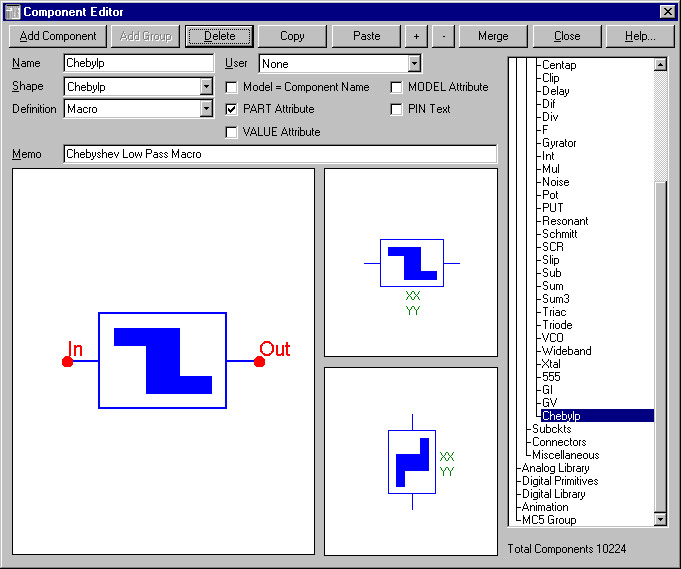
The Component Editor settings for the Chebyshev filter macro appear below. The name of the macro is the same as the macro circuit that was created, Chebylp. The Chebylp shape was created in the Shape Editor for this macro and signifies the basic low pass function of the filter. The definition for the component is stated as 'macro'. Two pins have been added to the shape. These are the In and Out pins which will link to the nodes labelled In and Out in the macro circuit.
|

|
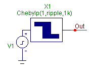
The filter macro is tested with the circuit below. This circuit is simply a pulse source that feeds into the input of the filter. The pulse source defaults to a 1V AC small signal source for AC analysis. The macro has its VALUE attribute defined as:
Chebylp(1,ripple,1k)
This defines the filter with a gain of 1 and a cutoff frequency of 1KHz. The ripple magnitude has been defined with the parameter 'ripple', and a corresponding .define has been placed in the text area of the circuit that states:
.define ripple 2
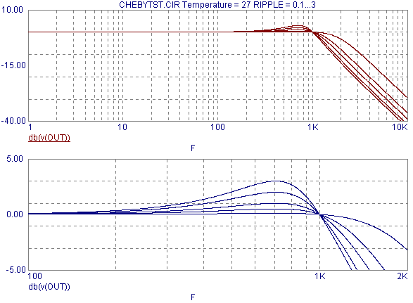
Chebyshev filters are characterized by their ripple response in the passband and a monotonically decreasing transmission in the stopband. The analysis below is the AC response of this filter. The symbolic parameter ripple has been stepped at the values of .1, .5, 1, 2, and 3 with the List option. This will step the magnitude of the ripple in the passband response. The top waveform shows the response from 1Hz to 10KHz of db(v(OUT)), and the bottom waveform zooms in on the ripple of the db(v(OUT)) waveform. As can be seen from the top plot, the gain in the passband is at 0dB and the cutoff frequency is at 1KHz.
|

|

|
|
|
|
|


