|
|
 |
Plotting Loop Gain Using the Tian Method
Loop gain simulations aid in determining the stability of a circuit by providing a method to measure the phase margin or the
gain margin of a circuit. Previous Spectrum Software newsletter articles in the Winter 2001 and Spring 1997 issues have
described methods for performing the loop gain calculation. This article will use the Tian method which is an improved
technique for measuring loop gain that was originally described in Reference 1.
There are two crucial items that must be adhered to in any of these loop gain simulation methods. First, the DC operating point
must not be affected by the method. Therefore, for the DC calculations, the loop must remain closed. Second, the user will need
to find a critical wire that the circuit can be opened at to perform this measurement. This critical point must be located at a
position where it would break all return loops in the circuit.
The Tian method uses a general two port analysis to calculate loop gain. There are at least three advantages to using the Tian method:
1) Less components need to be inserted into the circuit to calculate the loop gain.
2) The orientation of the components that make up the loop gain probe is not a factor. The orientation may be reversed and the
computations will remain the same.
3) The other loop gain methods such as the Middlebrook method assume that the feedback path is unilateral so the measurement is made in
only a single direction. The Tian method measures both the normal loop transmission and the reverse loop transmission. This is useful
when simulating at higher frequencies such as with microwave and RF applications.
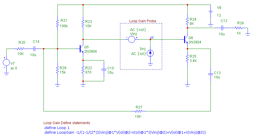
The circuit below was taken from Sedra and Smith and was also used as an example in the Winter 2001 issue.
|
|
The following steps need to be taken in order to use the Tian method with the circuit.
1) Zero out the AC magnitude in existing sources
Any Voltage Source or Current Source components that are present in the circuit should have their AC Magnitude parameter set to 0 so that they
create no signal during an AC analysis. In this example, the V7 voltage source is defined as:
AC 0
If there are any WAV File Source, Sine Source, or Pulse Source components in the schematic, these will need to be either disabled or deleted.
The AC magnitude of these sources are fixed at 1V. Note that this only refers to the components called Sine Source and Pulse Source, and not
the sine and pulse waveforms that can be defined within the Voltage Source and Current Source components.
2) Place the loop gain measurement components in the circuit
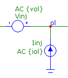
The loop gain measurement components then need to be placed at the critical point in the circuit where all return loops would be broken. The
components consist of just a Voltage Source and a Current Source as shown below.
|
|
The Voltage Source should be placed in series with the loop and have its PART and VALUE attributes defined as:
PART = Vinj
VALUE = AC {vol}
The DC value of the source defaults to 0V, so during the DC operating point calculation it behaves like a short circuit and the loop remains
closed. The Current Source should be placed at the plus side of the Voltage Source with its current flowing into the loop with the other side
of the source connected to ground. The Current Source needs its PART and VALUE attributes defined as:
PART = Iinj
VALUE = AC {iol}
At the junction between these two sources, the node should be given the node name "ol".
3) Place the loop gain define statements in the circuit
The following two define statements need to be placed in either the schematic or one of the text pages.
.define Loop 1
.define LoopGain -1/(1-1/(2*(I(Vinj)@1*V(ol)@2-V(ol)@1*I(Vinj)@2)+V(ol)@1+I(Vinj)@2))
The Loop variable will be stepped in the AC analysis in order to calculate the loop gain. The equation in the LoopGain variable was derived
by Frank Wiedmann from the Tian article. It uses the step selection operator, @, which is used to combine the waveform results from different
steps. For example, the following expression:
V(ol)@2
specifies the voltage at node ol during the second step of the simulation. Should the part names of the sources or the node name at the source
junction be different from those specified in the step above, then the LoopGain equation would need to be modified accordingly.
4) Place the If statement in the text page
The following If statement needs to be added to one of the text pages.
.if Loop==1
.define iol 0
.define vol 1
.elif Loop==2
.define iol 1
.define vol 0
.else
.define iol 0
.define vol 0
.endif
This If statement sets the values of the iol and vol variables depending on the value of the Loop variable. The iol and vol variables are used in
the voltage and current source in the loop gain probe. When the Loop variable is set to 1, then iol will be 0 and vol will be 1. When the
Loop variable is set to 2, then iol will be 1 and vol will be 0. All other values of Loop will set both iol and vol to 0.
For the Tian method, the AC analysis will go through two steps. In the first step, the voltage source is active and the current source is turned off
which corresponds to when the Loop variable is set to 1. In the second step, the voltage source is turned off and the current source is active which
corresponds to when the Loop variable is set to 2.
When running any other type of simulation, simply set the Loop variable to 0 in the define statement within the schematic to turn off both of these
sources.
5) Setup the AC analysis and stepping of the Loop variable
In the AC analysis limits, set the Frequency Range to the range that needs to be simulated. For the Y Expression fields, the following two waveforms can be plotted.
dB(LoopGain)
ph(LoopGain)
Both expressions use the equation set by the LoopGain define statement in the schematic. The first expression plots the loop gain response in decibels. The
second expression plots the phase of the loop gain response in degrees.
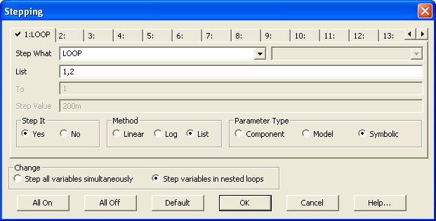
Next, the stepping of the Loop variable needs to be setup. In the Stepping dialog box, the symbolic variable Loop should be stepped between the values of 1
and 2. The easiest method to step the Loop variable in this manner is with the List method. Select the List option in the Method section. Set the List field to:
1,2
This will set the voltage and current sources to their appropriate values as specified within the If statement for each step of the simulation. It is important that the
Loop variable value be stepped in this specific order as the LoopGain equation has been defined based on this order. The complete settings for the stepping of the Loop
variable appear below.
|
|
The AC analysis results for the Sedra and Smith circuit are shown in the figure below. A performance tag has been added to the top plot to
display the phase margin of the simulation. The performance tag has been defined with the expression:
Phase_Margin(dB(LoopGain))
In order to use the Phase_Margin performance function, both the dB and phase waveforms of the expression LoopGain must be plotted. The resulting
phase margin of this simulation is calculated at 89.063 degrees so the circuit is safely within the stability requirement.
|
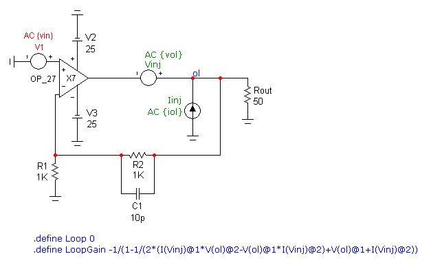
A second loop gain example is shown in the figure below. This circuit is measuring the loop gain response of an OP_27 low noise precision opamp.
|
|
There have been a couple of modifications from the Tian method described in the first example. First, rather than having the input source
to the circuit hardcoded as a zero volt AC stimulus, the V1 voltage source instead has its VALUE attribute defined as:
AC {vin}
Then the If statement in the text area has been adapted to include the vin variable used above as follows:
.if Loop==1
.define vin 0
.define iol 0
.define vol 1
.elif Loop==2
.define vin 0
.define iol 1
.define vol 0
.else
.define vin 1
.define iol 0
.define vol 0
.endif
The If statement now also sets the AC magnitude of the input source. For the loop gain calculations (when Loop is equal to 1 or 2), the vin
variable is set to 0. For any other value of Loop, the vin variable is set to 1.
The advantage to this modification is that the user no longer needs to manually edit the V1 source every time they go between an open loop
simulation and a closed loop AC simulation. In this case, the Loop define statement in the schematic is as follows:
.define Loop 0
Since the Tian method needs to have the Loop variable stepped which will override the value set in the schematic, simply enabling or disabling
the stepping of the Loop variable will now switch between the open loop and closed loop simulations.
In fact, with this setup, it is possible to plot both the open and closed loop response in the same simulation. In the Stepping dialog box, the
List field for the Loop variable is set to:
1,2,0
The first two values set the Loop variable to 1 and 2 for the first two steps which will perform the loop gain simulation as described with the
first circuit. The addition of the third value of 0 for Loop lets us plot the closed loop simulation too. Again, the order of the above values is
required to get the correct plots.
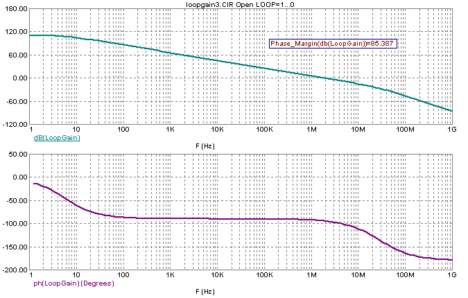
The resulting open loop simulation of the OP_27 circuit is shown below. The two waveforms plotted are:
dB(LoopGain)
ph(LoopGain)
A performance tag that displays the phase margin is in the top plot. The phase margin has been calculated at 85.387 degrees which is safely
within the stability requirement.
|
|
On a separate page of the AC analysis, the closed loop response is plotted using the following expressions:
dB(v(ol))@3
ph(v(ol))@3
These expressions plot the magnitude in decibels and the phase of the voltage at node ol. The step selection operator is set to plot only these
waveforms from the third step of the simulation. Since the Loop variable is set to 0 for the third step, the results display the closed loop
simulation. The closed loop simulation is shown in the figure below.
|
Reference:
1) "Striving for Small-Signal Stability", Michael Tian, V. Visvanathan, Jeffrey Hantgan, and Kenneth Kundert, Circuits & Devices, January 2001.
|
|
|
|
|


