|
|
 |
Schottky Diodes
A Schottky-barrier diode is fabricated by applying a metal contact to a moderately-doped n-type region. The underlying material can be silicon, or gallium-arsenide. The junction produced by the metal, which behaves like a lightly-doped p-type material, and the moderately-doped n-type material, is a rectifying diode-like contact. It differs from ordinary diode junctions in two important ways:
Switching is faster
The Schottky diode achieves current transport by movement of majority carriers, as opposed to normal diodes, which employ minority carriers. This produces a very fast diode due to the drastic reduction in the usual charge storage effects associated with minority carriers.
Voltage drop is lower
The forward drop of the Schottky diode is much smaller than that of normal diodes, being on the order of 0.3v to 0.5v for silicon and around .7v for gallium-arsenide Schottky diodes.
Modeling a Schottky diode is done using the standard diode primitive. The main objectives are to match the low forward I-V characteristic and the fast switching time.
The normal forward drop of the diode with typical parameters is about 0.7 volts for currents in the 10m to 100ma range. In a Schottky diode the drop will be somewhat lower. Typically the forward drop is around .3 to .5 volts. To achieve the lower drop you can increase the diode IS model parameter value from its typical value of 1E-15 to as high as 1E-9. The larger the IS the smaller the forward drop.
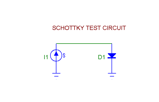
To illustrate the effect of the IS parameter, consider the following test circuit.
To simplify the process, consider the following test circuit.
|

|
|
This circuit contains a current source which drives the diode under test to display the forward characteristic in DC analysis. It also is programmed to emit a current pulse in transient analysis to display the transit time delay. The diode's IS is set to 1n, its N is set to .5, and its TT is set to 10p.
Select DC analysis from the Run menu. The DC analysis limits look like this:
|
These analysis limits are set to logarithmically sweep the current source from 1pa to 100ma. The log step factor of 1.5 means to multiply each value of I1 by 1.5 until the final value of 1e-10 is achieved. The expression fields are set up to plot the diode's current versus its voltage so that we can see the diode's forward IV curve.
|
Here is the Stepping dialog box. It specifies that we are to step the diode's IS parameter from 1E-14 to 1E-10. For each value of IS one complete DC analysis sweep will be done producing one IV curve, so we can see the effect of the IS parameter on the diode's forward characteristic.
This is what the run looks like:
|
You can achieve a similar curve by reducing the N value and using a normal (1E-15) value for IS. Here is an example where the IS parameter is set to 1E-15 and N is varied from .3 to .5 resulting in a forward drop in the same range. Here the diode forward drop at 50ma varies from 250mv at N=.3 to about 420mv when N=.5.
|
To illustrate how to measure the TT time, we'll run transient analysis on this circuit. The pulse source has been set up to produce a forward biasing current, then a reverse biasing current and we are interested in the time it takes the diode to come out of forward bias. Here are the transient analysis limits.
|
These analysis limits are set to plot the source current and the diode voltage so that we can measure the reverse transit time.
|
Here is the Stepping dialog box. It specifies that we are to step the diode's IS TT linearly from 100P to 500p. For each value of TT one complete transient analysis run will be done producing one plot of the diode voltage, so we can see the effect of the TT parameter on the diode's reverse transit time.
This is what the run looks like:
|
The plot shows that for the case of a 1u forward and 1u reverse current pulse, the reverse transit time is about 2/3 of the TT parameter. Estimating the necessary TT value then is fairly easy. For Schottky diodes, the reverse transit time is usually from 100p to 500p, so setting the TT value to half this value is a good quick approximation.
|
|
|
|
|


