|
|
 |
NTC7 Test Signal
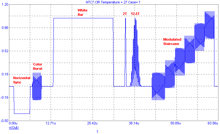
Video testing is performed by placing a known test signal at the input of the system and observing the output to see if there is any distortion. If the system can pass the signal with little or no distortion, then it will be able to pass a picture signal as well. One such test signal is the NTC7 composite test signal. The NTC7 signal provides a user with multiple video-system testing opportunities. The white bar is used for testing insertion gain and distortions in medium time waveforms. The 2T pulse is used for testing distortions in short-time waveforms. The 12.5T pulse tests for luminance-chrominance delay disparities. Finally, the modulated staircase tests the differential gain and differential phase errors.
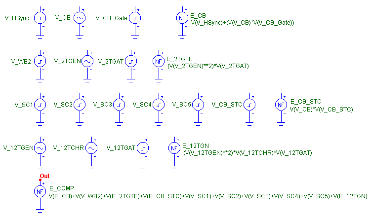
To create this signal in Micro-Cap, multiple voltage sources must be used. The schematic below displays one configuration of sources that can be used to create the NTC7 test signal. This configuration was created based on an article by Anthony Radice, titled "Spice Simulations Use Controlled Sources to Model NTSC Signals" which appeared in the March 1, 1991 issue of EDN. This schematic can easily be turned into a macro for use in other schematics.
|

|
Note that for all of the following sources that use model statements, both the PART attribute and the MODEL attribute have been defined with the same name, and that the period for the NTC7 test signal is assumed to be 63.56us. For this signal, volts represent IRE levels. 0V would be the blank level (0 IRE) and 1V would be the white level (100 IRE). The negative going horizontal sync pulse is created by the V_HSync pulse source. This source uses the following model statement:
.MODEL V_HSYNC PUL (VONE=-0.4 P1=1.4u P2=1.6u P3=6.3u P4=6.5u P5=63.56u)
The model creates -0.4V pulse with 0.2us rise and fall times and a width of 4.7us. Otherwise, the voltage level of the pulse will be zero volts. The color-burst signal is created from a combination of the V_CB sine source and the V_CB_Gate pulse source. This signal refers to 9 cycles of a 3.58MHz subcarrier that provides a reference for the color phase and the color saturation level. The V_CB sine source creates a sine wave with a 0.2V peak amplitude and a frequency of 3,579,545Hz, and the V_CB_Gate pulse source produces a 1V pulse for 2.6us starting at 7.2us. These sources use the following model statements:
.MODEL V_CB SIN (F=3579545 A=.2)
.MODEL V_CB_GATE PUL (VONE=1 P1=7u P2=7.2u P3=9.8u P4=10u P5=63.56u)
The nonlinear fuction voltage source, E_CB, then proceeds to multiply the V_CB and V_CB_Gate signals together. When multiplied, the pulse source zeroes out the sine source for all but the 2.6us where the pulse source has a value of 1V. This gates the sine source generator and produces the appropriate color burst. In addition to producing the color bust, the E_CB function source also adds the horizontal sync and the color burst together. The entire VALUE attribute for the E_CB source is:
V(V_HSync)+(V(V_CB)*V(V_CB_Gate))
The white bar is created by the V_WB2 pulse source. This source creates a 1V (100 IRE) pulse that starts at 13.6us and lasts for 18us. For the rest of the signal, it is at 0V. The V_WB2 source uses the model statement:
.MODEL V_WB2 PUL (VONE=1 P1=13.4u P2=13.6u P3=31.6u P4=31.8u P5=63.56u)
The 2T pulse is created from a combination of the V_2TGEN sine source, the V_2TGAT pulse source, and the E_2TGTE function source. The 2T pulse has a sin squared characteristic and a pulse width equal to two periods of the 3.58MHz chroma subcarrier which is used in the color burst. This characteristic can be simulated by squaring a 1V sine source that has a frequency of 894,886Hz. Squaring the sine source produces voltage levels between 0V and 1V at a frequency of 1.79MHz. The peak of this pulse should be centered on 35.4us. In order to do this, the sine source must have a phase shift. For the center to be at this time, the sine source must be crossing 0V at exactly 35.1255us. Since one period of the sine source is 1.117us, the phase shift for the sine source can then be calculated to be 244 degrees. The V_2TGAT pulse source then gates the V_2TGEN sine source by simulating a 1V pulse starting at 35.1265us for .559us which covers exactly one period of the squared sine source. The two model statements used by these sources are:
.MODEL V_2TGEN SIN (F=894886 PH=3.543)
.MODEL V_2TGAT PUL (VONE=1 P1=35.1255u P2=35.1265u P3=35.6835u P4=35.6845u
+ P5=63.56u)
Note that the phase parameter in the sine source has been converted into its radian equivalent. The E_2TGTE function voltage source is used to square the sine source and then multiply the result by the gating pulse source to produce the 2T pulse. The VALUE attribute for the E_2TGTE source is defined as:
(V(V_2TGEN)**2)*V(V_2TGAT)
The 12.5T modulated pulse is created from a combination of the V_12TGEN sine source, the V_12TCHR sine source, the V_12TGAT pulse source, and the E_12TGN function source. This pulse has a sin squared characteristic and a width equal to 12.5 periods of the 3.58MHz chroma subcarrier. The envelope of this pulse is created in the same manner as the 2T pulse where, in this case, a 1V sine source with a frequency of 143,182Hz is squared to produce the 0V to 1V amplitude and a frequency of 286,364Hz. The peak of the 12.5T pulse should be centered at 38.4us so a phase shift for the sine source needs to be calculated. Since the period of the sine source is 3.492us and the zero crossing must occur at 36.654us, then the phase can be calculated to be 89 degrees. The modulating sine source for the 12.5T pulse is a 3.58MHz sine souce. Since the source should be between 0 IRE (0V) and 100 IRE (1V), both the DC component and the amplitude of this source should be set to .5V. The V_12TGAT pulse source is used to gate the pulse. It produces a 1V pulse starting at 36.655us that will last for 3.49us. The model statements for these three sources are as follows:
.MODEL V_12TGEN SIN (F=143182 PH=1.553343)
.MODEL V_12TCHR SIN (F=3579545 A=.5 DC=.5)
.MODEL V_12TGAT PUL (VONE=1 P1=36.654u P2=36.655u P3=40.145u P4=40.146u
+ P5=63.56u)
Again, the phase for the sine source has been converted into its radian equivalent. The E_12TGN function source is then used to square the V_12TGEN signal and multiply the result by the two other sources to produce the final 12.5T modulated pulse. The VALUE attribute for this source is defined as:
(V(V_12TGEN)**2)*V(V_12TCHR)*V(V_12TGAT)
The last stage of this signal is the modulated staircase. This portion of the signal can be regarded as six bursts of the chroma that was also used for the color burst. The center for each step of the staircase is 18 IRE (.18V) higher than the previous step, rising to a maximum of 90 IRE (.9V) with the sixth step. The staircase is created from a combination of the V_CB sine source, the V_SC1 to V_SC5 pulse sources, the V_CB_STC pulse source, and the E_CB_STC function source. Since the phase of the chroma should be 0 degrees and the amplitude .2V, the chroma can be taken from the V_CB sine source which was described earlier in the article. This source provides the modulation for the staircase. The V_SC1 to V_SC5 pulse sources provide the center voltage for each of the steps in the staircase. The modulated staircase has six steps, but since the first step is centered around 0V, only five pulse sources are needed. Note that the timing of the pulse sources overlap each other so that there is an additive effect on the base level of the chroma signal. Each pulse source has an amplitude of .18V and occurs 3us after the previous step began thus creating the staircase effect. The V_CB_STC pulse source provides a gating signal for the V_CB chroma signal. It produces a 1V pulse starting at 43.4us and lasting for the entire 19us that the modulated staircase lasts for. The model statements for all of these pulse sources are as follows:
.MODEL V_SC1 PUL (VONE=.18 P1=47.4u P2=47.41u P3=62.41u P4=62.42u P5=63.56u)
.MODEL V_SC2 PUL (VONE=.18 P1=50.4U P2=50.41U P3=62.41U P4=62.42U P5=63.56U)
.MODEL V_SC3 PUL (VONE=.18 P1=53.4U P2=53.41U P3=62.41U P4=62.42U P5=63.56U)
.MODEL V_SC4 PUL (VONE=.18 P1=56.4U P2=56.41U P3=62.41U P4=62.42U P5=63.56U)
.MODEL V_SC5 PUL (VONE=.18 P1=59.4U P2=59.41U P3=62.41U P4=62.42U P5=63.56U)
.MODEL V_CB_STC PUL (VONE=1 P1=43.4u P2=43.41u P3=62.41u P4=62.42u
+P5=63.56u)
The E_CB_STC function source is then used to multiply the V_CB chroma signal and the V_CB_STC gate signal which zeroes out the chroma signal except for the 19us needed for the staircase. The VALUE attribute defined for the function source is:
V(V_CB)*V(V_CB_STC)
Finally, the E_COMP function source is used to add all of the different components of the NTC7 composite signal together. The VALUE attribute for this source is defined as:
V(E_CB)+V(V_WB2)+V(E_2TGTE)+V(E_CB_STC)+V(V_SC1)+V(V_SC2)+V(V_SC3)
+V(V_SC4)+V(V_SC5)+V(E_12TGN)
The + sign that begins the second line above is not a continuation character in this case but is actually used for addition.
The final simulation result of the NTC7 composite signal is displayed below. Since the signal is dependent on phase shifts to produce the 2T and the 12.5T pulses, it is only reliable over a single period of simulation.
|

|
|
|
|
|


