|
|
 |
Using Global Nodes
In a schematic, it is a common occurrence for multiple components to share the same power supply. When all of the power supply pins are on the main level, it is easy to wire the pins together or label each pin with the same node name which will connect them together without wiring. If the schematic is a multiple level schematic, it is easier to use a global node to connect the power supply pins rather than trying to wire them together. Micro-Cap has the capability to define any node as a global node which will make it accessible by all subcircuits or macros without having to be passed as a parameter argument. A global node is defined by giving the node a name in the following format:
$G_name
The $G_ at the beginning of the node name signifies to Micro-Cap that this node is to be treated as a global node. For a schematic, entering a node name is done by going into Text mode, and then clicking on the node. When the text dialog box comes up, type in the node name and hit OK. When a piece of text is used as a node name, a pin connection will be placed on the node where the bottom left corner of the text touches the node. For a subcircuit, simply edit the node name in the text file so that it has the above format.
|

|
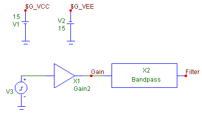
The schematic above gives an example of the use of global nodes. The circuit consists of a pulse source that is input to a gain macro whose output goes into a bandpass filter subcircuit. As seen in the figure, neither the gain stage nor the bandpass filter stage have any external power pins. In the upper left of the schematic are two batteries. These two batteries have their non-ground nodes labelled as $G_VCC and $G_VEE. Due to the global naming of the nodes, the two voltages of the batteries are accessible in any level of the schematic.
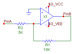
The schematic below is the macro circuit for the gain macro. The circuit contains an opamp in the standard inverting gain of two configuration. The key to this macro is that the positive and negative supply pins on the opamp component have been labelled using the global node names, $G_VCC and $G_VEE. Since the power supplies are global, the nodes PinA and PinB are the only nodes that need to be passed to the main circuit.
|

|
The bandpass filter subcircuit models a Butterworth bandpass filter with a gain of 0dB. It has
a 20dB stopband attenuation with a center frequency of 1KHz, a passband of 100Hz, and a
stopband of 400Hz. This filter was created through the Active Filter Designer in Micro-Cap, and
then converted to a SPICE listing with the Translate to SPICE file option. The subcircuit
consists of the following listing:
	.SUBCKT   BANDPASS   IN   OUT
	C1  0  1  CM1  10.02506N
	C2  1  3  CM1  10.02506N
	C3  0  8  CM1  10.02506N
	C4  8  9  CM1  10.02506N
	R1  1  In  RM1  641.46204K
	R2  0  3  RM1  23.29013K
	R3  0  4  RM1  31.32138K
	R4  6  4  RM1  90.83004K
	R5  1  6  RM1  23.29013K
	R6  0  1  RM1  24.1676K
	R7  8  6  RM1  597.59976K
	R8  0  9  RM1  21.69758K
	R9  0  10  RM1  29.17967K
	R10  Out  10  RM1  84.61921K
	R11  8  Out  RM1  21.69758K
	R12  0  8  RM1  22.51505K
	X1  3  4  $G_VEE  6  $G_VCC  UA747C
	X2  9  10  $G_VEE  Out  $G_VCC  UA747C
	*
	.MODEL  RM1  RES  (R=1  LOT=1%)
	.MODEL  CM1  CAP  (C=1  LOT=1%)
	.ENDS
	*  OPAMP
	*  PINS:    1=NC+  2=NC-  3=VEE  4=VO  5=VCC
	.SUBCKT  UA747C  1  2  3  4  5
	C1  6  7  8.66025e-012
	C2  12  13  3e-011
	CE  10  14  1e-019
	D1  18  19  D
	D2  20  18  D
	D3  4  16  D
	D4  17  4  D
	D5  3  5  D
	E1  14  0  POLY(2)  5  0  3  0      0  0.5  0.5
	F1  13  14  POLY(5)  VS1  VC  VE  VLP  VLN  0  4.24413e+007  -4.24413e+007
	+  4.24413e+007  4.24413e+007  -4.24413e+007
	GA  12  0  6  7      0.000188496
	GCM  0  12  10  0      5.96075e-009
	H1  18  0  VS2  1000
	IEE  10  3  1.516e-005
	Q1  6  2  8  QINN
	Q2  7  1  9  QINP
	R2  12  11  100000
	RC1  5  6  5305.16
	RC2  5  7  5305.16
	RE1  8  10  1837.31
	RE2  9  10  1837.31
	RE  10  14  1.31926e+007
	RO2  13  14  25
	ROUTAC  15  4  50
	RP  5  3  18165.2
	VC  5  16  1
	VE  17  3  1
	VLN  0  20  25
	VLP  19  0  25
	VS1  11  0  0
	VS2  13  15  0
	*
	.MODEL  D  D  ()
	.MODEL  QINN  NPN  (BF=83.3333)
	.MODEL  QINP  NPN  (BF=107.143  IS=1e-016)
	.ENDS  UA747C
The bandpass filter subcircuit calls a second subcircuit, the UA747C opamp, within it. The calls to the UA747C subcircuit are the lines that start with X1 and X2. Two of the nodes in each of these calls are defined as the global nodes, $G_VCC and $G_VEE. These nodes in the call correspond to the positive and negative power supply pins from the opamp subcircuit.
Due to the labelling of the global nodes, the batteries in the main circuit provide the power for the opamp in the gain macro circuit, and the two opamps that are called within the bandpass subcircuit. One very nice result of this is that the power supply for the entire circuit is easily changed by simply editing the batteries on the main circuit.
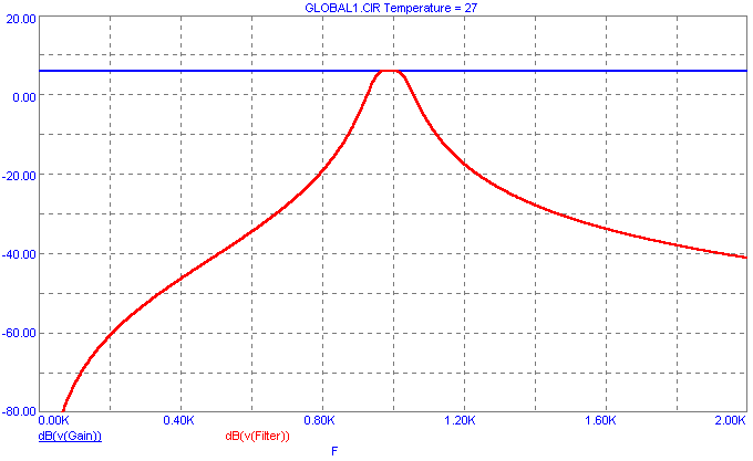
The AC analysis simulation of the main circuit appears below. The circuit has been simulated from 0Hz to 2KHz. Two waveforms have been plotted. These waveforms are the gain in dB at the output of the gain macro, and the gain in dB at the output of the filter. The gain from the gain macro is a constant 6.02dB over this frequency range as can be expected from an amplifier with a gain of 2. The gain from the filter shows the bandpass characteristics of the filter at the 1KHz center frequency.
|

|
|
|
|
|


