|
|
 |
Common Digital Mistakes
Not Initializing Flip-Flops or Latches
One common mistake in using digital flip-flops or latches is the failure to initialize the part. For many configurations, not initializing a flip-flop or latch won't cause a problem, but for some toggle and counter configurations, it will produce undesired results.
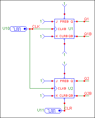
The circuit below has two JK flip-flops that are set up to run in toggle mode having both the J and the K inputs set to 1. Both flip flops share the same clock, and both have Fixed Digital components defined as 1 at the Prebar, J, and K inputs. The only difference between the two flip-flops is that the top flip-flop has its Clrbar input fixed to the 1 state, and the bottom flip-flop has a digital stimulus going into its Clrbar input. This digital stimulus has its Command attribute specified as:
0 0 55ns 1
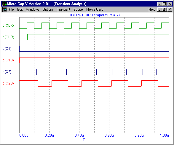
which produces a 0 state for the first 55ns of the simulation, and then is at a 1 state for the rest of the simulation. This will initialize the Q2 output of the flip-flop to the 0 state. The analysis below displays the transient results of this schematic for a run of 1us. The bottom flip-flop, which has been initialized to 0, is toggling correctly as shown by waveforms D(Q2) and D(Q2B). The outputs of the top flip-flop, which have not been initialized, are at an X, unknown, state for the entire simulation as shown by waveforms D(Q1) and D(Q1B). The reason for this is that the default initialized state of a flip-flop or a latch is the X state. When the negative edge of the clock occurs, the flip-flop is toggled, but toggling an X state can only produce the same X state by definition.
A way to initialize all flip-flops and latches in a schematic without having to place a set or clear pulse on each part is to set the DIGINITSTATE parameter that is available in the Global Settings. A 0 sets all flip-flops and latches to the 0 state, a 1 to the 1 state, and a 2 to the X state.
|
|
|
Using Open Collector Parts without Pullup Components
Another common mistake occurs when using an open collector output as the input to another digital device. When used in conjunction with other digital devices, an open collector part needs to have a digital pullup component placed on each of its outputs.
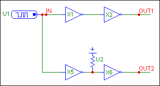
The circuit below displays a schematic that has a digital stimulus feed two 7405 open collector output inverters. Each of these open collector outputs is then passed on as the input to a 7404 inverter, which has standard outputs. The only difference between the top section and the bottom section is that the bottom section has a digital Pullup component connected to the output of its 7405. The pullup component has its I/O MODEL attribute defined as IO_PULLUP. This I/O model is then defined in the text area as:
.MODEL IO_PULLUP UIO (DRVH=1K DRVL=1Meg)
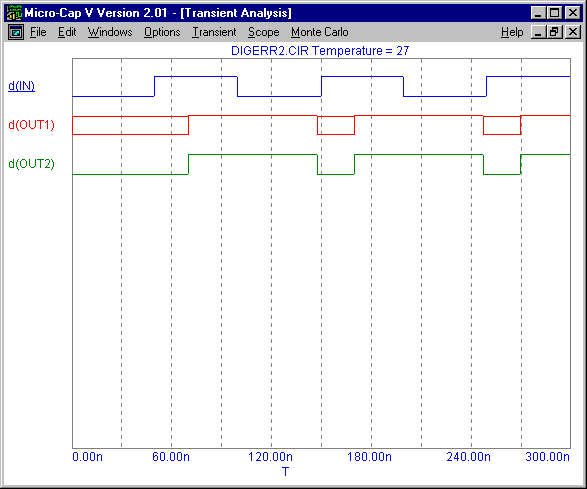
This model is setup assuming that only digital components will be connected to the node. Otherwise, specific AtoD and DtoA subcircuit models would need to be created for the I/O model. Whenever the node it is connected to is 1, it models a 1 kohm pullup resistor, but when the node is 0, it is essentially an open circuit. Since the output of the inverter is open collector, the pullup is supplying the driving impedance whenever the output is high. The analysis below displays the results of a transient analysis for this circuit. The waveform D(OUT2) is as expected. The waveform D(OUT1) has an X state whenever a 0 state is expected. This is because there is no digital pullup on the output of the 7405. That 7405 output is unable to drive the 7404 whenever the output is 1 due to the high impedance of the node and this causes the unknown state at OUT1.
In setting DRVH for the I/O model, make sure that the impedance won't dominate any other outputs connected to the node and that it is lower than the value set for DIGDRVZ in the Global Settings.
|
|
|
Rise and Fall Conflicts in Mixed Mode Simulation
When running a mixed mode simulation, there are transition states produced between the 0 and 1 states. These states are the R (rise) and F (fall) states. These states signify the uncertainty of the transition. For example, standard TTL components are guaranteed to be at a 0 state below .8V and at a 1 state above 2V. Somewhere in this 1.2V gap is the actual transition between the 0 and 1 states. The R and F states represent the digital state in this voltage gap. They imply that the digital node has transitioned from 0 to 1, for a rise state, or from 1 to 0, for a fall state, at some point during this state, though the exact time is unknown.
This uncertainty can cause conflicts with edge triggered flip-flops. For a positive edge triggered flip-flop, if the D input is at an R or F state when the positive edge of the clock occurs, the outputs of the flip-flop will transition to an X state. The reason for the X state output is that the R and F states represent a state where the node may be either 0 or 1 at any given time so the output must be unknown since the input is not specifically known.
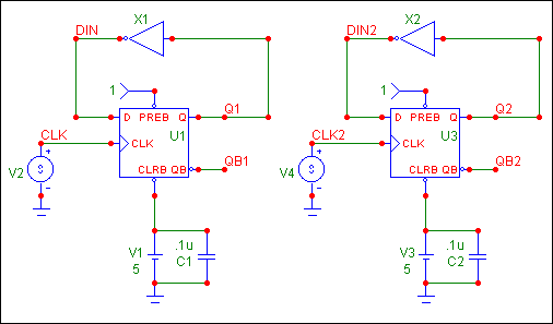
The figure below displays a schematic that produces this conflict. The left circuit is identical to the right one except for one attribute. The IO_LEVEL attribute on the right flip-flop has been set to 2 instead of the default 0. This forces the flip-flop on the right to use the level 2 I/O models that only produce 0 and 1 states, so that there will be no R and F conflicts. The left flip-flop uses the default level 1 I/O models.
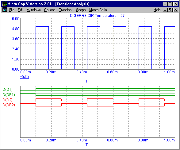
The analysis below displays the transient results for this schematic. The D(Q2) and D(QB2) waveforms produce the expected results due to the fact that they are using the level 2 I/O models. The D(Q1) and D(QB1) waveforms use the level 1 I/O models and upon the first positive clock edge, the outputs transition from a 0 to an X. At this edge, the clock's transition is 0-R-1. When the clock turns to an R state, the output is then set to an R state. This R state then goes through the feedback to the D input. When the clock finally hits its 1 state, the D input is now R, and the output is then set to X.
Unknown states flag areas of the simulation where there may be a conflict and that the user may need to look into more. Conditions that may cause these problems are long rise and fall times of analog pulses and undesired propagation delays on a feedback loop. In this circuit, changing the rise time in the V2 pulse source from .1us to .05us will also produce the expected results. However, the conflicts are not always desirable in all simulations. Individual digital primitives may have their I/O model levels changed through their IO_LEVEL attribute. The default 0 in this attribute forces the component to use the setting specified by the Global Setting DIGIOLVL. The DIGIOLVL parameter in the Global Settings can globally control the I/O model level. Setting the parameter to 1 uses the level 1 I/O models and 2 uses the level 2 I/O models.
|
|
|
|
|
|
|


