|
|
 |
Z Domain Simulation
The Z transform is a means to mathematically describe a sampled data system. The Z transform is given by the following equation:

z-n is a delay operator, n is the number of previous unit delays, T is the sampling interval, and V(nT) are the discrete analog samples. This equation cannot be represented directly in MC5. MC5 can run its equivalent Laplace transform though. With a Laplace function source, any z domain transfer functions may be converted to a Laplace transfer function through the substitution:
z=exp(sT)
One of the common uses of z transforms is to simulate discrete-time systems such as digital and switched capacitor filters. The following example is adapted from an article by B. Al-Hashimi and M. Moniri in the April 11, 1996 edition of EDN titled "Spice provides z-domain circuit simulation." This example simulates a third order, elliptic, lowpass switched-capacitor filter. This filter is represented by the following z domain transfer function.
H(z) = (0.10285(z+1)(z*z-0.70621z+1))/((z-0.55889)(z*z-1.1579z+0.76494))
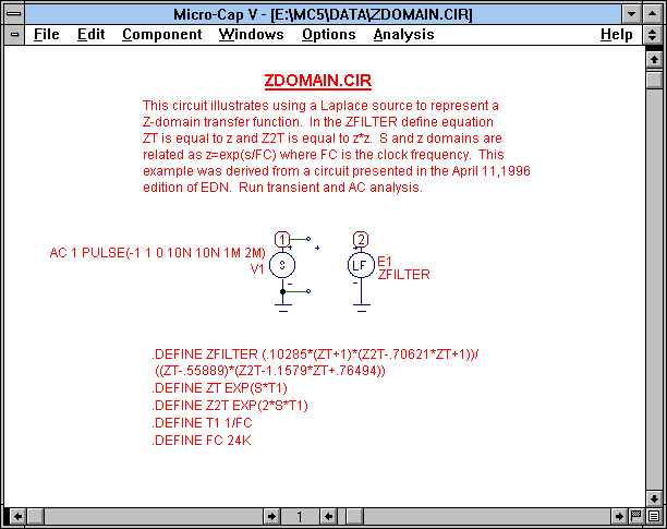
The figure below displays the MC5 equivalent circuit.
|
|
The circuit contains two components. One is the SPICE independent source, V, that provides the input stimulus, and the other is a Laplace function VofV source which represents the switched capacitor filter. The V source is defined as a 1ms pulse with 10ns rise and fall times and a 2ms period for transient analysis. For AC analysis, it is defined as an AC small signal source of magnitude 1V. The Laplace source's Laplace attribute is given the name ZFILTER. ZFILTER is defined through the following five .define statements.
.DEFINE ZFILTER (.10285*(ZT+1)*(Z2T-.70621*ZT+1))/
+ ((ZT-.55889)*(Z2T-1.1579*ZT+.76494))
.DEFINE ZT EXP(S*T1)
.DEFINE Z2T EXP(2*S*T1)
.DEFINE T1 1/FC
.DEFINE FC 24K
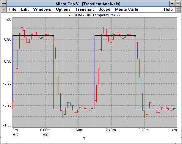
In the above define statements, FC is the clock frequency value whose reciprocal is the sampling interval, T1. T is not used as the variable in this case due to a conflict with the time variable, T. ZT is defined as the Laplace equivalent of z, and Z2T is defined as the Laplace equivalent of z*z. Finally, the transfer function is included in the define statement for ZFILTER. The + on the second line of the ZFILTER define statement is a continuation character and has no effect on the equation. The figure below displays the transient results of this circuit. The transient analysis clearly shows a sampling interval of 41.6us.
|
|
Using Transmission Lines as the Z Domain Delay Element
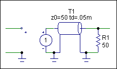
A second method for simulating a Z domain transfer function is to implement the 1/z terms with ideal transmission lines. The transmission line equivalent of 1/z appears in the figure below.
|
|
The transmission line is specified by its characteristic impedance, ZO, and its propagation delay time, TD. The TD parameter represents the sampling interval of the digital filter. The value of the characteristic impedance is not important as long as the line is terminated by a resistor of equal value. The source at the input of the transmission line is just a VofV dependent source with a gain of 1. This is just a buffer to isolate the 1/z elements when they are placed in series.
To demonstrate the use of the transmission line for Z domain analysis, we will analyze a third order Butterworth digital filter. The transfer function for the digital filter is as follows:
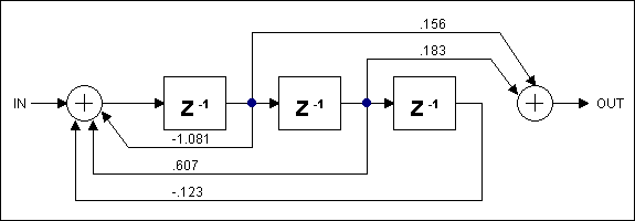
H(z) = (.156/z+.183/z*z)/(1-1.081/z+.607/z*z-.123/z*z*z)
Below is the corresponding block diagram. With the use of transmission lines, the block diagram becomes an easier tool to design from rather than the transfer function. This diagram was created using Micro-Cap's graphic elements.
|
|
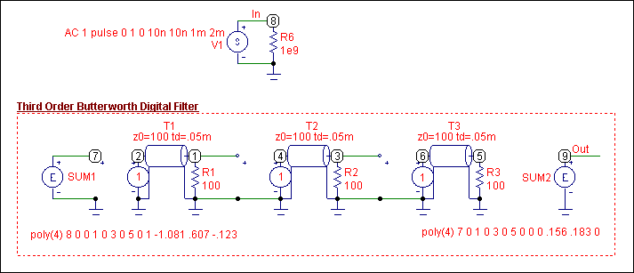
The block diagram above is simulated by the circuit below.
|
|
The input to the filter is again a 1ms pulse in transient analysis and a 1V AC small signal source in AC analysis. For each 1/z element, one of the transmission line blocks has been placed in the circuit. Going from left to right, these produce the 1/z, 1/z*z, and 1/z*z*z delays. Each transmission line has ZO defined as 100 ohms, with a corresponding 100 ohm resistor terminating the line. The TD parameter of the transmission lines has been defined in order to give the filter a 20kHz sampling frequency.
The other two elements in the filter are EVofV SPICE dependent sources. These represent the two sum nodes that appear in the block diagram. These two sources sum all of the elements specified by the block diagram together by using the POLY operator. The POLY operator performs the following function:
POLY(4) 8 0 0 1 0 3 0 5 0 1 -1.081 .607 -.123
is equal to
0+V(8,0)*1+V(0,1)*(-1.081)+V(0,3)*.607+V(0,5)*(-.123)
SUM1 defines the sum at the input, and SUM2 defines the sum at the output. For a typical transfer function such as:
H(z) = (b0+b1z-1+b2z-2+b3z-3)/(1+a1z-1+a2z-2+a3z-3)
the POLY sources would be defined as:
SUM1: POLY(4) IN 0 0 Z-1 0 Z-2 0 Z-3 0 1 a1 a2 a3
SUM2: POLY(4) SUM1 0 Z-1 0 Z-2 0 Z-3 0 0 b0 b1 b2 b3
where IN is the input node number, Z-1 is the node number at the output of the first delay element, Z-2 is the node number at the output of the second delay element, Z-3 is the node number at the output of the third delay element, and SUM1 is the node number at the SUM1 element.
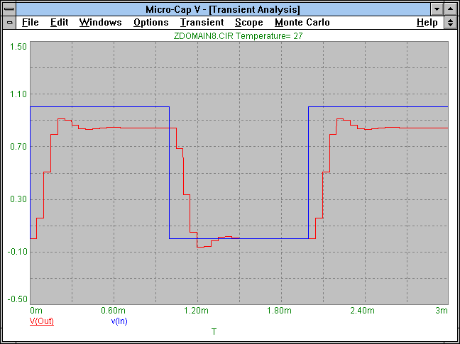
The transient analysis of this circuit is shown below. In the transient analysis, note the 50us sample intervals of the V(Out) waveform.
|
|
|
|
|
|


