|
|
 |
Changing the Power Supplies of Digital Parts
The default power supplies of all digital parts in MC5 is set at 5V. In many applications, these supplies must be adjusted for accurate simulation. There are a few methods for changing the power supplies which are dependent on whether it is local or global, on what type of digital family that is to be changed, and on whether it is a digital primitive or a subcircuit. Currently, there are two power supply subcircuits contained in the DIGIO.LIB (digital input/output library): one for the 74/TTL families and one for the CD4000 family. One thing to keep in mind when changing the power supplies is that all of the components in the digital library have their propagation delays and constraint times defined in accordance with 5V operation. Editing the digital library may be a necessity if the delays or constraints are a factor in the simulation.
Changing the Default Power Supply
The two default power supply subcircuits appear below:
*****74/TTL POWER SUPPLY SUBCIRCUIT*****
.subckt DIGIFPWR AGND
+ optional: DPWR=$G_DPWR DGND=$G_DGND
+ params: VOLTAGE=5 REFERENCE=0
V1 DPWR AGND {VOLTAGE}
R1 DPWR AGND 1E9
V2 DGND AGND {REFERENCE}
R2 DGND AGND 1E9
R3 AGND 0 1m
.ends
*****CD4000 POWER SUPPLY SUBCIRCUIT*****
.param CD4000_VDD=5V
.param CD4000_VSS=0V
.subckt CD4000_PWR AGND
+ optional: VDD=$G_CD4000_VDD VSS=$G_CD4000_VSS
+ params: VOLTAGE={CD4000_VDD} REFERENCE={CD4000_VSS}
V1 VDD AGND {VOLTAGE}
R1 VDD AGND 1E9
V2 VSS AGND {REFERENCE}
R2 VSS AGND 1E9
R3 AGND 0 1m
.ends
The method to edit these supplies is simple. First of all, open the
DIGIO.LIB file that is present in the DATA subdirectory. Find the power
supply subcircuits in the file. For the 74/TTL power supply subcircuit,
you only need to edit the line that begins with '+ params:' and place in
the appropriate value for the VOLTAGE parameter. The REFERENCE parameter
is by default 0V and may also be changed. The new line should appear similar
to:
+ params: VOLTAGE=3.3 REFERENCE=0
For the CD4000 power supply subcircuit, edit the lines that begin with
'.param'. These two .param statements control the supply rails.
CD4000_VDD controls the positive power supply and CD4000_VSS controls the
ground or negative supply. The edit should appear similar to:
.param CD4000_VDD=15V
There are a couple of drawbacks to this method. The first one is that this changes the value used by all circuits that reference the default value. Any circuits that have been created previously would now use the new value which may not be desired. Using one of the older circuits would require changing the DIGIO.LIB back to its original values or to edit the circuit using one of the other methods mentioned in this article. The second drawback only occurs with the 74/TTL power supply subcircuit. Some of the families that reference this subcircuit, such as the LS family, are only designed to be run at 5V. Changing the power supply would cause these parts to run incorrectly when placed in a mixed mode configuration.
Changing the Power Supply for all CD4000 Parts in a Circuit
Instead of changing the default value, the CD4000 family offers a simple way to change the power supply of all CD4000 components in a single circuit. Notice how in the CD4000 power supply subcircuit there were the two '.param' statements. These statements set the default value in the DIGIO.LIB file. However, if a '.param' statement is present in the schematic, it will override the values present in the DIGIO.LIB file. Therefore, to change the power supply for the circuit, all one has to do is add the following statement either in the schematic or in the text area.
.param CD4000_VDD=10V
All of the CD4000 components in this circuit would then use a single 10V supply.
Using Separate Power Supplies in a Circuit
Sometimes, there may be a need to have separate power supplies for digital parts in one circuit. In this case, a new power supply subcircuit and a new I/O model statement will need to be created. The best way to do this is to copy the appropriate power supply subcircuit and I/O model to a new file, so that it won't be overwritten in the case of an upgrade. You can use these as shells to easily create new ones. The example we are going to use is to create a 3.3V power supply for the 74HC family. The new power supply will appear as follows:
.subckt DIGPWR3V AGND
+ optional: DPWR=$G_DPWR DGND=$G_DGND
+ params: VOLTAGE=3.3 REFERENCE=0
V1 DPWR AGND {VOLTAGE}
R1 DPWR AGND 1E9
V2 DGND AGND {REFERENCE}
R2 DGND AGND 1E9
R3 AGND 0 1m
.ends
The only changes made from the 74/TTL power supply subcircuit is the name of the subcircuit and the VOLTAGE parameter value.
The new I/O model for the 3.3V HC family appears below:
.model IO_HC_3V uio (
+ DRVH=50 DRVL=50
+ INLD=3p
+ ATOD1="ATOD_HC" ATOD2="ATOD_HC_NX"
+ ATOD3="ATOD_HC" ATOD4="ATOD_HC_NX"
+ DTOA1="DTOA_HC" DTOA2="DTOA_HC"
+ DTOA3="DTOA_HC" DTOA4="DTOA_HC"
+ TSWHL1=3.472ns TSWHL2=3.472ns
+ TSWHL3=3.472ns TSWHL4=3.472ns
+ TSWLH1=3.209ns TSWLH2=3.209ns
+ TSWLH3=3.209ns TSWLH4=3.209ns
+ DIGPOWER="DIGPWR3V")
The only changes made from the IO_HC model were the name of the model and the value of the parameter DIGPOWER. Note that the DIGPOWER parameter now contains the name of the power supply that was just created. Minor adjustments may need to be made on the impedances and the switching times, but the changes above will give you a solid model for simulation.
Place the name of the new library in the Nom.lib file, found in the DATA subdirectory, in the same format that all of the other libraries appear. You need to do this so that MC5 can access the library through its internal .lib statement. To use this new model, you would place IO_HC_3V into the I/O MODEL attribute of a digital primitive or if using one of the subcircuits from the digital library, you would replace all instances of IO_HC with IO_HC_3V throughout the subcircuit. Any other HC parts can still access the IO_HC model that would give them a 5V power supply.
Using an On Schematic Power Supply with a Digital Primitive
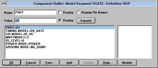
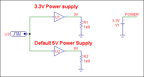
Having a digital primitive access a power supply that exists on the schematic is as simple as changing one of its attributes. Each primitive has two attributes that control the power supply nodes. The two attributes are POWER NODE and GROUND NODE. By default, these are set to $G_DPWR and $G_DGND which are the nodes that are produced by the 74/TTL power supply subcircuit. These attributes may be set to any nodes that exist in the schematic. Below is the Attribute dialog box of the U1 part from the schematic below. The POWER NODE attribute references the Power node that is at the top of the 3.3V battery.
|

|
The node number itself may also be used in the attribute, but naming the node is a better procedure since the node numbers may change if the circuit is edited. The schematic has two identical buffers except that one references a 3.3V power supply and the other references the default 5V power supply. The resistors have been added to be able to view the analog voltage display.
|

|
Using an On Schematic Power Supply with a Digital Subcircuit
The power and ground nodes of all components in the digital library have been defined as optional nodes such as in the following subcircuit header.
.SUBCKT CD4009UB A ABAR
+ OPTIONAL: VDD=$G_CD4000_VDD VSS=$G_CD4000_VSS
+ PARAMS: MNTYMXDLY=0 IO_LEVEL=0
The VDD node is the power node and the VSS node is the ground node. The OPTIONAL keyword lets you add one or more nodes to the subcircuit call. If the nodes are included in the circuit, they override the default node values which in this case are derived from the CD4000 power supply subcircuit.
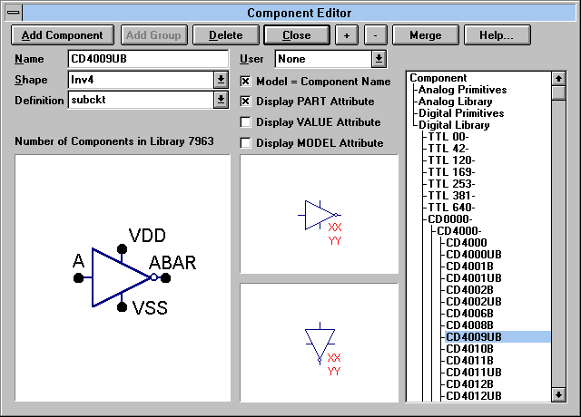
In order to include these nodes in a schematic, the pins VDD and VSS must be added to the component in the Component Editor. The figure below displays the modified CD4009UB part within the Component Editor. The shape for the CD4009UB was changed to Inv4 so that it would have power and ground leads. Clicking in the Shape area of the Component Editor lets you add pins to the shape. The VDD and VSS pins were added and specified as analog pins since the power supply subcircuit consists only of analog components. The power and ground nodes are now ready to be accessed in a schematic.
|

|
The figure below shows a sample circuit using the CD4009UB. If the VDD and VSS pins are added, they must be connected to either a voltage source or ground. The simulation simply steps the V1 battery from 5V to 15V in 5V increments and views the voltage waveform at the Out node.
|
|
|
|
|


