|
|
 |
Changing the Power Supplies of a Digital Library Part
All of the components within the Digital Library have a default power supply defined for them. These default power
supplies are defined within the I/O model that is assigned to each component. The I/O models for all of the digital
parts that come with Micro-Cap can be found in the Digio.lib library file in the Library folder. For some digital
families, the I/O model has been created to only handle a single power supply value such as 5V for the standard TTL
devices. In other families, the I/O model can handle a range of power supply values. For example, the I/O model for
the CD4000 series can handle power supplies ranging from 3V to 15V. The default power supply for the CD4000 series
is 5V. One method for changing the default power supply that is assigned to a part from the digital library can be
accomplished using a combination of global nodes and the OPTIONAL attribute.
The example in this article will use the CD4000 series of devices to demonstrate how to modify the power supply for
a single device in the schematic. However, the CD4000 series also has a unique method of setting the default power
supply for all of the CD4000 devices that are in the schematic. To change the power supply for all of these devices
in the circuit, all one has to do is add the following statement either on a schematic page or in a text page.
.param CD4000_VDD=10V
All of the CD4000 components in this circuit would then use a single 10V supply. However, if the schematic contains
CD4000 components that operate at different power supplies, then a different technique must be used to define the
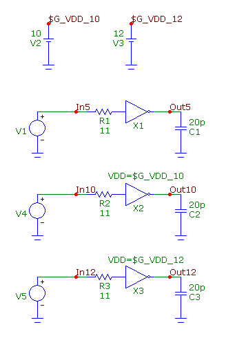
power supply for a single component. A simple example of such a circuit is shown in the figure below.
|

|
The circuit consist of three CD4049B inverters. Each inverter will operate on a different power supply.
One will use the default 5V supply, and the other two will use a 10V and a 12V supply.
The first step is to create the power supplies on the schematic. In this case, the V2 battery has been
defined to model the 10V supply, and the V3 battery has been defined to model the 12V supply. Text has
been added to the output of these batteries in order to name the node. The 10V supply node has been
named $G_VDD_10, and the 12V supply node has been named $G_VDD_12. Note that both of these node names
begin with $G_. The use of the $G_ prefix declares that these nodes are global nodes. Global nodes are
nodes whose names are globally available to all parts of the circuit, including the top level circuit and
all macros and subckts used by it. A global node name must be used for the power supply node as that is
the only method to connect the supply node to the underlying subcircuits that make up the corresponding
I/O model for the digital device.
The next step is to look at the subcircuit header for the digital device model. The header can be viewed
by double clicking on the device in the schematic to invoke the Attribute dialog box. In the text area
at the bottom of the dialog box, the subcircuit model will be shown. Below is the subcircuit header for
the CD4049B device.
.SUBCKT CD4049B INA OUTA
+ Optional: VDD=$G_CD4000_VDD VSS=$G_CD4000_VSS
+ params: MNTYMXDLY=0 IO_LEVEL=0
Within the header, there is an Optional keyword that declares optional nodes that may be connected externally
to the subcircuit. For the digital library parts, the positive and negative power supply nodes are always
declared within this Optional keyword. For the CD4049B model, the VDD and VSS nodes are the optional nodes
and by default, they are connected to the global nodes $G_CD4000_VDD and $G_CD4000_VSS that are defined within
the I/O model for this device.
The easiest method to connect optional nodes in a subcircuit to a supply in the schematic is to use the
OPTIONAL attribute available in the Attribute dialog box. Since the X1 inverter is using the default 5V
power supply, the OPTIONAL attribute for that component is left blank. The X2 inverter will use the 10V
power supply, so it has its OPTIONAL attribute defined as:
VDD=$G_VDD_10
This overwrites the default node specified within the subcircuit header, so that the VDD node for the inverter
is now connected to the $G_VDD_10 global node defined in the schematic. The X3 inverter will use the 12V power
supply so it has its corresponding OPTIONAL attribute defined as:
VDD=$G_VDD_12
This connects its VDD node to the $G_VDD_12 global node in the schematic.
For the inverters in the schematic, the VSS node will continue to be connected to the default $G_CD4000_VSS which is just a grounded node.
When an analysis is entered, Micro-Cap will automatically connect the corresponding power supplies to any AtoD or
DtoA interfaces that have been added to the circuit internally.
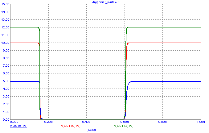
A 1us transient simulation is run on the circuit. Each inverter has the exact same external circuitry. The only
difference lies within the power supply reference and the magnitude of the input pulse. The resulting transient
simulation is shown below.
|

|
The plot shows the output at each of the inverters. When the output of the inverter is at a one
state, the analog voltage is dependent on the power supply assigned to the device. As expected,
these inverters produce analog output voltages that correspond with the power supply voltage that
they are using.
For the CD4000 devices, the .Param statement can also be used in conjunction with the OPTIONAL
attributes. For example, in the schematic, if a couple of CD4000 devices were to operate at 10V,
but the rest of the CD4000 devices were operating at 12V, simply place the following .param statement
in the schematic:
.param CD4000_VDD=12V
Then add a 10V power supply to the schematic that uses a global node name, and define the OPTIONAL attributes
for those devices that are to operate at 10V. The .Param statement overwrites the default setting for all
of the CD4000 devices, but then the OPTIONAL attribute overwrites the .Param setting for those specific instances.
|
|
|
|
|


