|
|
 |
Using the Bus
The bus capability within Micro-Cap provides a convenient method for transporting multiple
signals while limiting the clutter of having multiple wires in the schematic. The bus
is most useful for digital circuitry where related sets of signals are often routed
through the same areas of the schematic such as with a memory or data set.
The bus is easy to implement in the schematic. It requires the use of two modes: Bus
mode and Wire mode. The Bus mode is used to create the connectors that retrieve the
individual signals from the bus wire. The Wire mode creates the bus wire that links
the bus connectors. This article will describe the process of using a bus in a
schematic.
|
 |
Bus mode toolbar icon |
 |
Wire mode toolbar icon |
| |
The circuit used in this example will be a simple digital circuit. The circuit takes
a pair of four-bit digital signals and inputs them to a 7483A adder. Both of the
four-bit signals along with their sum from the output of the adder are input into
7448 BCD to seven segment decoders. This is an ideal situation to use the bus as
the four-bit data sets are routed together throughout the circuit. Although this
example consists of digital nodes, analog nodes can also be linked through the bus
in the same manner. The digital circuit using standard wires to transport the signals
is shown below.
|
Even on a simple circuit such as this, it takes a little bit of effort to track the
paths of the signals. Using the bus will greatly enhance the readability of the
schematic. The first step is to delete all of the existing wires in the schematic as
they will all be replaced with buses. The circuit without any wiring appears below.
|
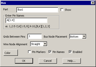
The first step in creating a bus is to place a bus connector. A bus connector is
created by first enabling Bus mode. Clicking in the schematic when in Bus mode
invokes the Bus dialog box shown below.
|
|
The Bus dialog box lets you define the individual pin names of the connector along with
the location and spacing of the bus node and wire nodes. The main entries in the dialog
box are as follows:
Part: This field contains the bus connector name. The name has no effect on the
simulation.
Enter Pin Names: This field sets the pin names, implicitly defining the number
of separate wire nodes for the bus connector. The pin names determine the connectivity
of the bus. For example, a pin named A1 will be connected to any other pins named A1
that are on other connectors that share the same bus wire. The names can be listed
separately or using the following forms.
A,B,C,D - A four pin bus with pins labeled A, B, C, and D
A[1:4] - A four pin bus with pins labeled A1, A2, A3, and A4
C[1:4,8,9] - A six pin bus with pins labeled C1, C2, C3, C4, C8, and C9
0:7 - An eight pin bus with pins labeled 0, 1, 2, 3, 4, 5, 6, and 7
[A,B][1,2] - A four pin bus with pins labeled A1, A2, B1, and B2
Grids Between Pins: This specifies the number of schematic grids between pins.
Bus Node Placement: This specifies where to place the bus connector. There are
three options; top, middle, and bottom.
Wire Node Alignment: This specifies how the wires will emerge from the
connector. The wires may be set to straight, slanted up, or slanted down.
Creating the Buses
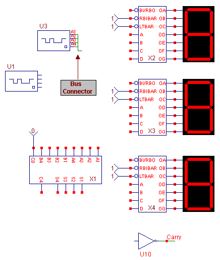
The first bus added to the circuit will connect pins from the U3 stimulus source,
the X1 7483A adder, and the X2 7448 decoder.
First, enable Bus mode. Then click in the schematic by the U3 component. The Bus
dialog box will appear. Define the pin names as A[1:4] which will create a four pin
connector with pins named A1, A2, A3, and A4. Set the Grid Between Pins as 1, Bus Node
Placement as Bottom, and Wire Node Alignment as Straight. Hit OK. The bus connector
will appear in the schematic. The connector can be moved or rotated just like any
other component. Move and rotate the connector so the four wire nodes connect directly
to the pins of the stimulus source. The bus node should be at the bottom of the
device. The circuit should look like the schematic below.
|
|
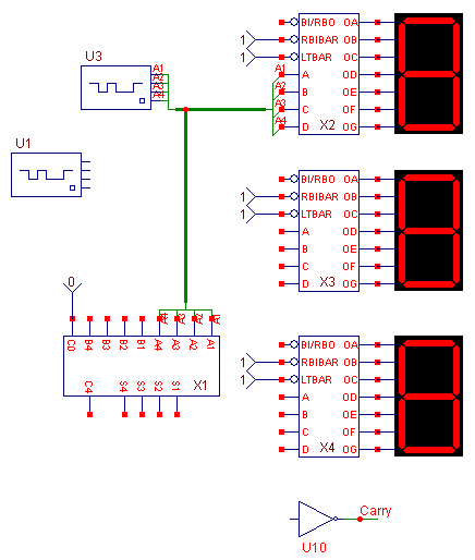
Now we will add the bus connector for the X2 device. In Bus mode, click once again in the
schematic to invoke the Bus dialog box. Define the pin names as A[1:4] so it shares the
same signals as the first connector. Set the Grid Between Pins as 2, Bus Node Placement
as Middle, and Wire Node Alignment as Up. Hit OK. Rotate and move the component so
that the wire nodes of the bus connector connect to the A, B, C, and D inputs of the
decoder. The A1 pin of the connector should connect to the A input of the
decoder.
The third connector for this bus will go to the X1 adder. In Bus mode, click in the
schematic. Set the Grid Between Pins as 2, Bus Node Placement as Middle, and Wire
Node Alignment as Straight. Hit OK. Rotate and move the component so that the wire
nodes of the connector connect to the A1, A2, A3, and A4 inputs of the adder. The A1
pin of the connector should connect to the A1 input of the decoder.
Now it is time to wire the connectors together. Enable Wire mode. Drag a wire from
the bus node of the first connector to the bus node of the second connector. The bus
wire is displayed on the schematic with a thicker width than the standard wire to
visually denote that it is a bus wire. Now drag another wire from the bus node of
the third connector up until it connects to the existing bus wire. The bus wires
connect in the same manner as standard wires do. Note that bus wires cannot connect
to anything but the bus nodes of the bus connectors or to other bus wires. The results
should appear similar to the circuit below. Bus connector pins that share both
the same pin name and the same bus wiring will be connected together. For example, the
output of the U3 stimulus source that goes into the A3 pin is connected to the C input
of the X2 decoder and the A3 input of the X1 adder.
|
|
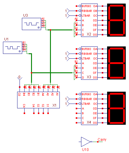
The second bus will connect pins from the U1 stimulus source, the X1 7483A adder, and
the X3 7448 decoder. The pin names for this set of connectors will be defined as
B[1:4] which will create four pin connectors with pins named B1, B2, B3, and B4.
Since these connectors will be on a different bus wire than the first set of
connectors, we could have used A[1:4] again, but in practice, it is better to have a
different set of pin names for each bus. Using the same technique and other settings
used to create the first bus, the three bus connectors are then added to the schematic
and wired together. The results appear below.
|
|
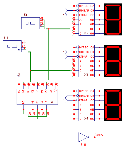
The third bus will connect the outputs of the adder to the inputs of the X4 decoder
and U10 inverter. In Bus mode, click below the adder. Define the pin names as O[1:5]
which will create a five pin connector with pins named O1, O2, O3, O4, and O5. Set the
Grid Between Pins as 2, Bus Node Placement as Middle, and Wire Node Alignment as
Straight. Hit OK. In this case, we will move the connector so it is near the pins of
the adder but not directly connected to it. Then we will use standard wires to connect
the bus connector pins to the adder pins. The O1 pin should connect to the S1 adder
output, and the O5 pin should connect to the C4 adder output. The circuit should look
similar to the schematic below.
|
|
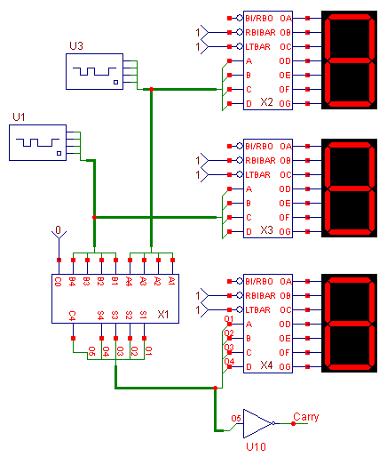
Now we will add the bus connector for the X4 device. In Bus mode, click in the
schematic to invoke the Bus dialog box. Define the pin names as O[1:4]. Since
only the S1 to S4 outputs of the adder are needed as inputs for this decoder, the
bus connector only uses the pin names that were connected to those signals with
the other connector. Set the Grid Between Pins as 2, Bus Node Placement as Bottom,
and Wire Node Alignment as Up. Hit OK. Rotate and move the component so that the
wire nodes of the bus connector connect to the A, B, C, and D inputs of the decoder.
The O1 pin of the connector should connect to the A input of the decoder.
The inverter just needs a single signal off of the bus. In Bus mode, click in the
schematic. Define the pin names field as O5. This will input the C4 signal from
the adder into the inverter once the bus is wired. The Grid Between Pins is not
relevant with just a single pin so leave it at 2. Set the Bus Node Placement as
Middle and Wire Node Alignment as Up. Hit OK. Rotate and move the component so
that the O5 pin is connected to the inverter input.
Finally, wire the bus nodes of these three connectors together. The final schematic
appears as below. Note that to further clean up the schematic, the pin names were
hidden on the connectors for the first two buses. The pin name display is controlled
by double clicking on a connector when in Select mode and enabling or disabling the
Pin Names checkbox. Comparing the final schematic to the original schematic with the
individual wires gives a clear demonstration on how using the bus can improve the
readability of a schematic.
|
|
|
|
|
|


